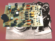

At least one such amplifier project appeared in aX(1), but it retained a fairly high number of discrete transistors between the composite op amp input stage and the output section, perhaps for good reason. I did not build the four amplifiers shown in this article, but I did run a SPICE simulation to verify that they did perform as audio amplifiers. I provided the circuits, showing waveforms at selected points in the circuitry, as a basis for further experimentation. I selected the feedback values to provide a −3dB frequency response of 2Hz to 86kHz at a gain of 20 (26dB), with a sprinkling of other parts, where necessary, to provide adequate loop stability and avoid excessive phase shift or response peaking.
I simplified the drawings by using diode bias, so in a real-world amplifier the output transistor bias must be optimized with the usual Vbe multiplier bias-spreading transistor. I also do not show components such as output device protection circuits, the zobel network for the speaker, RF oscillation suppression, and power supply filter and decoupling caps. Output devices are yours to select, as are the op-amps unless otherwise specified.

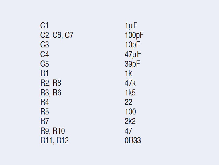
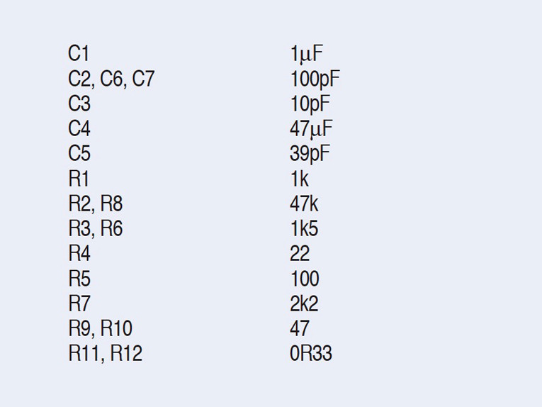
Figure 1 shows the simplest circuit using an op amp for the gain stage, with the simulation part values in Table 1. The emitter-follower output transistors are inside the op amp feedback loop. The same supply voltage as the op amp powers the output stage, so the absolute maximum power supply voltage specified for the op amp and its output voltage swing limits the output power.
Most audio-quality op amps have an absolute maximum supply limit of ±18V DC. Applying a derating factor of 90%, the maximum safe supply reduces to about ±16V DC. Higher voltage op amps are available, such as the older NE5532 and NE5534A, which have ±22V DC absolute maximum limits, allowing almost ±20V DC for the rails. In what is a happy coincidence, one of the highest quality audio op amps, the OPA604 and its dual OPA2604, have the highest absolute maximum power supply limit of ±25V DC, allowing a safe rail supply of ±22.5V DC.
Since the OPA604 output swing is limited to 3V below the supply rails, the voltage drive to the output devices is limited to ±19.5V, or about 14V RMS at the speaker. This delivers more than 23W into an 8Ω load, and may serve your audio purposes quite well. Indeed, the Monarchy Audio SM-70 Pro 25Wpc power amplifier uses a hybrid OPA2604 IC op amp/discrete MOSFET design (2).
The circuit in Fig. 1 is called a current-boosted op amp. If you need more output power, you will require additional voltage gain beyond the limited output voltage swing from the op amp.
Current And Voltage Amplifiers
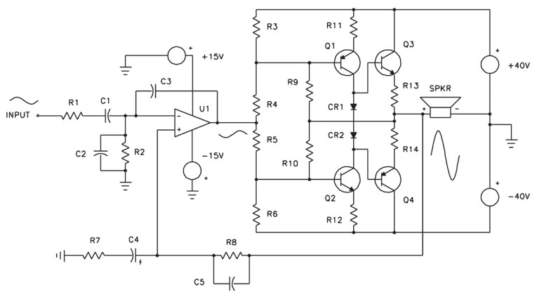
The hybrid amplifier in Fig. 2 is from a Linear Technologies application note (3). The app note circuit is an inverting amplifier designed to deliver ±120V into 6k, so I modified it for non-inverting gain and the higher current, lower voltage output a loudspeaker requires.
Common-emitter transistors Q1 and Q2 provide the voltage gain to the emitter follower output stage Q3 and Q4, which provides current gain. Q1 and Q2 cause a signal inversion, so the op amp is configured as an inverting amplifier to make the overall power amplifier non-inverting. The negative feedback connection looks strange, because it needs to be brought to the non-inverting input.
Since the op amp power supply rails no longer limit the output voltage swing, you can employ any high-quality audio op amp. The added complication is the need for a lower voltage supply for the op amp. You can easily obtain this from the ±40V output supply via linear regulators.
When you operate the output devices as source-followers or emitter-followers, as in Fig. 1, there is no possibility for output stage oscillation, since the gain of any follower stage is always less than one. With a common-source or common-emitter
amplifier, the output device gain and phase shift provide an increased opportunity for oscillation or ringing, so careful frequency compensation takes a high priority.
An Unusual Design
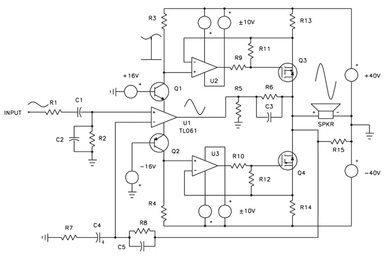
Figure 3 shows a unique method, employed by Velleman in their K4020 stereo power amplifier (4). Again, the circuit is greatly simplified, and you could easily implement the MOSFET output stage with bipolar transistors. The pre-amplified input signal is sent to the non-inverting input of U1, a TL061 low-power op-amp. This is not a low-noise, low-distortion device like the TL070-TL074. I selected it for its low power supply current (250μA versus 2.5mA for the TL071).
Here’s where the design becomes unusual. The ±15V supply for the TL061 comes from the emitter of an NPN (Q1) and a PNP (Q2) transistor whose bases are connected to +16V and −16V supply rails, respectively. Each transistor has a collector load resistor, connected to the high-voltage MOSFET supply rail, in what resembles a cascode connection. The emitter current in each transistor is equal to the TL061 supply pin current, which, in turn, is a composite of the op amp quiescent current and the amplified audio signal into loading resistor R5 at the output of the TL061.
An FET-input op-amp, whose non-inverting input is connected to the collector of its “cascode” transistor, drives the gate of each output MOSFET. The split supply for each op amp floats and is referenced to the high-voltage supply rail for its respective MOSFET. Local feedback comes from the source terminals, across R13 and R14 source resistors. Thus each op amp drives its MOSFET gate such that its source operates at the same voltage seen at the “cascode” transistor collector. At idle, the 250μA supply current to the TL061 sets the bias in each MOSFET.
Each common-source MOSFET produces gain in the output stage according to the ratio of the source resistor to the speaker load impedance. Resistor R15, in case of an open speaker terminal, also loads the MOSFET drains. As with the Fig. 2 amplifier, the common-source stage gain and phase shift provide an increased opportunity for oscillation or ringing. There are two feedback loops from the output stage back to the TL061. Conventional overall negative feedback is taken from the output drains back to the inverting input of U1. Then there is additional feedback through a parallel network consisting of R6 bypassed by C3, from the output drains to load resistor R5.
The obvious disadvantage of Fig. 3 over Fig. 2 is the need for three op amps and four separate split power supplies. Normally, in a complementary symmetrical split-supply amplifier, the negative terminal of the speaker is grounded (Figs. 1−3), while the amplifier output stage drives the positive terminal. This is called a driven speaker configuration. Since the power section always has less than unity voltage gain, the output power in a driven speaker design sourced by an op amp will be limited by the relatively low swing of the op amp (Fig. 1). However, some modern guitar amplifiers (5−7) use opamps for the front-end voltage gain stage and obtain added voltage gain with an interesting configuration.

Driven Supply
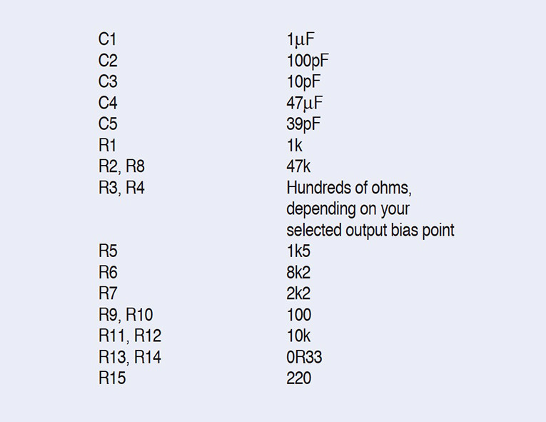
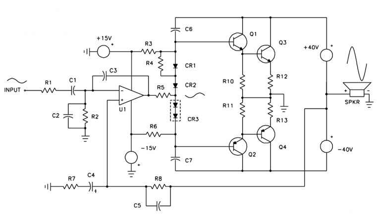
In Fig. 4, the ±40V DC power supply common point is left floating. If you ground emitter resistors R12 and R13 of complementary output transistors Q3 and Q4 and connect the speaker + to the floating power supply center-tap, the voltage across the speaker can swing by approximately the full ±40V DC power supply voltage. This is called the driven supply configuration. During the positive input half-cycle, transistors Q2 and Q4 are turned on (op-amp U1, connected as an inverting amplifier, has a negative output). Current flow through Q4 causes the center tap of the floating power supply to swing positive, producing a positive half-cycle across the speaker. During the negative input half-cycle, Q1 and Q3 turn on, with opposite results.
With a ±40V DC power supply, the peak speaker voltage at full power can be roughly ±37V, driving 26V RMS or 84W into an 8Ω load. Yet the output of U1 need only swing by Vout/gain, or ±1.8V for a voltage gain of 21 (26dB). This completely eliminates the need for a high voltage VAS transistor. It does complicate the design of the op-amp power supply, however. The ±40V DC supply is not referenced to ground, but the op-amp ±15 supply must be. Either a separate transformer winding is required for the ±15V DC supply, or it must be “sampled” and stored in large capacitors from the high voltage supply rails as they swing up and down at audio frequencies.
Although the output stage appears to be an emitter-follower, it is a common emitter amplifier since the emitter resistors are grounded. The ratio of the speaker impedance to the emitter resistors realizes the voltage gain. The earlier caveats concerning the care needed to ensure stability apply here as well. As with the Fig. 2 amplifier, feedback must return to the non-inverting input of U1. I hope these hybrid op amp/discrete power amplifier topologies give you some ideas for your own designs.
This article was originally published in audioXpress, July 2003.
References
1. “A 50W/Channel Composite Amplifier,” Kenneth Miller, audioXpress, April ’01, p. 7. (available online - click the title)
2. “Product Review: Monarchy Audio SM-70 and SE-100 Delux Power Amplifiers,” Gary Galo, Audio Electronics 5/00, p. 28; “Product Review: Monarchy Audio SM-70 Pro Power Amplifier,” Gary Galo, audioXpress, Sept. ’01, p. 66.
3. “Power Gain Stages for Monolithic Amplifiers,” Jim Williams, Linear Technology Corp. Application Note AN18, Fig. 9, p. 7. See www.linear.com (Linear is now part of Analog Devices)
4. “Kit Review: Velleman K4020 Amplifier,” Charles Hansen, Audio Electronics 5/99, pp. 38-47. See www.vellemanstore.com.
5. U.S. Patent 5,197,102 “Audio Power Amplifier with Frequency Selective Damping Factor Controls,” 1993, Jack Sondermeyer; Peavey Electronics Corp. See www.peavey.com.
6. U.S. Patent 5,524,055 “Solid State Circuit for Emulating Tube Compression Effect,” 1996, Jack Sondermeyer; Peavey Electronics Corp.
7. U.S. Patent 5,796,305 “Amplifier Arrangements with High Damping Factor,” 1998, Jack Sondermeyer; Peavey Electronics Corp.
Note
Peavey mentioned that although they do utilize the “driven supply” circuit in many of their amplifiers, and have for years, they were not the first to do so. Jack Sondermeyer said he was not the person to come up with the idea. In talking to some of their folks, they first remember this type of circuit in an early Sunn amplifier, circa 1970 or so.