
LFPAK33 devices also feature a significantly lower resistance responding to growing industry pressure to reduce the size of modules in the car while continuing to improve energy efficiency and reliability. The Nexperia LFPAK33 package uses a copper clip design to reduce the package resistance and inductance which in turn reduces the RDS(on) and losses of the MOSFET. The resulting package has an ultra-compact footprint of 10.9 mm2, and because no wires or glue is used internally, operating temperatures of up to 175oC Tj max are possible. Devices can handle up to 70 A, and the extensive product portfolio includes devices that range between 30 V – 100 V and an RDS(on) as low as 6.3 mΩ.
“As more subsystems are crammed into cars the need for rugged, compact power systems is becoming ever greater,” said Richard Ogden, International Product Marketing Engineer at Nexperia. “This extension of our LFPAK portfolio provides designers with more product choices than anywhere else on the market today.”
Target applications include: connected auto modules, next generation engine management systems; chassis and safety technology; LED lighting; relay replacement; C2X, radar, infotainment and navigation systems; and ADAS.
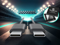
 EMI and ESD Protection for USB 3.1 Type C, HDMI 2.0 and MIPI M-PHY Systems in a Single Compact Package
Nexperia also announced three new series of common mode EMI filters with integrated ESD protection: PCMFxUSB3S, PCMFxHDMI2S and PESDxUSB3S, which provide support for USB 3.1 Type C, HDMI 2.0 and MIPI M-PHY interfaces. Using the same footprint, Nexperia’s TrEOS ESD protection diodes are offered in the same package. System engineers will benefit from having a single device instead of two (common mode filter plus TrEOS ESD protection component) saving PCB space and improving reliability and design flexibility. With both solutions available in the same package, designers can determine at a late stage whether they need to include EMI filtering at all without being concerned about PCB layout spins. Also, the same board layout will be suitable for all markets, whether filtering is required or not. Furthermore, the new integrated common mode filters feature an extremely wide differential passband of more than 6 GHz.
Nexperia’s TrEOS ESD protection technology delivers extremely low capacitance to maintain excellent signal integrity, low clamping voltage/dynamic resistance to protect the system chip, and high ESD and surge ruggedness. By using active silicon-controlled rectification, none of these parameters are compromised. The result is an extremely fast turn-on time of about 0.5 ns that enables devices to withstand up to 20 kV contact discharge. This exceeds level 4 of the IEC 61000-4-2 standard.
Stefan Seider, product manager at Nexperia, comments, “Portable devices such as smartphones are getting smaller, requiring transmission standards such as Wi-Fi, Bluetooth and LTE together with USB3.1 data frequencies. Our combinational PCMF filters are a highly efficient solution as they are the only devices available on the market to offer both ESD protection and EMI filtering in a single package with the same footprint as ESD-only protection diodes, both for USB 3.1 data rates. Therefore, Nexperia offers the best RF performance, common mode rejection at the critical frequencies and ESD clamping, and designers can change between common mode filters with ESD and ESD-protection-only without changing the footprint.”
www.nexperia.com