 As most of our customers know, I have been advocating the advantages of FETs in general and JFETs in particular, especially for low and medium level circuits. JFETs provide extremely high resolution, bringing out more details, sounding cleaner, clearer, and more natural than the best bipolar transistors such as the LM394, and even the best Telefunken tubes. Overall, I believe the JFETs offer the best sound in audio circuits.
I have been working with JFETs since the middle of the ’70s, when I developed low-level amplifier modules with JFETs at Motorola. However, they were not competitive with the best bipolars at that time. In the early ’80s came the first really low-noise, high-gm devices on the market. I have used these devices in the input stages of practically all my designs since then. However, I use bipolar transistors in the second stages, mostly because they offer a fairly simple design.
The output stages have always been MOSFETs, because of the relatively high current required in these stages. In the ever-continuing quest for better sound, I have reviewed my designs regularly, improving the topology of the amplifiers and also using better components, thus bringing significant improvements. However, I first achieved a real breakthrough when I started to use mostly JFETs in the amps. It is my considered opinion that it would be best to use only JFETs in all stages of the audio chain. However, due to their limited power-handling capability, it is practically impossible to use them in output stages. Here, MOSFETs will rule for the foreseeable future.
In spite of their quadratic characteristics and relatively high input capacitance, JFETs are fairly simple to use in audio amplifiers, and you, as an amateur, can design most low-level stages in an audio chain yourself. Just like a single vacuum tube triode or pentode, a single JFET can handle the task of a line amp, and it is significantly simpler to hook up. You can also build a single-ended (SE) phono stage with only two JFETs. The rest is up to your imagination. Suffice it to say that I hope the following introduction to JFETs will whet your appetite for the “new frontiers” in audio amplification.
JFETs
Field-effect transistors (FETs) have been around for a long time; in fact, they were invented, at least theoretically, before the bipolar transistors. The basic principle of the FET has been known since J.E. Lilienfeld’s US patent in 1930, and Oscar Heil described the possibility of controlling the resistance in a semiconducting material with an electric field in a British patent in 1935. Several other researchers described similar mechanisms in the ’40s and ’50s, but not until the ’60s did the advances in semiconductor technology allow practical realization of these devices.
The junction field-effect transistor, or JFET, consists of a channel of semiconducting material through which a current flows. This channel acts as a resistor, and the current through it is controlled by a voltage (electric field) applied to its gate. The gate is a pn junction junction, formed along the channel. This description implies the primary difference between a bipolar transistor and a JFET: the pn junction in a JFET is reverse-biased, so the gate current is zero, whereas the base of a bipolar transistor is forward-biased, and the base conducts a base current. The JFET is therefore an inherently high-input impedance device, and the bipolar transistor is comparatively low-impedance.
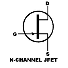
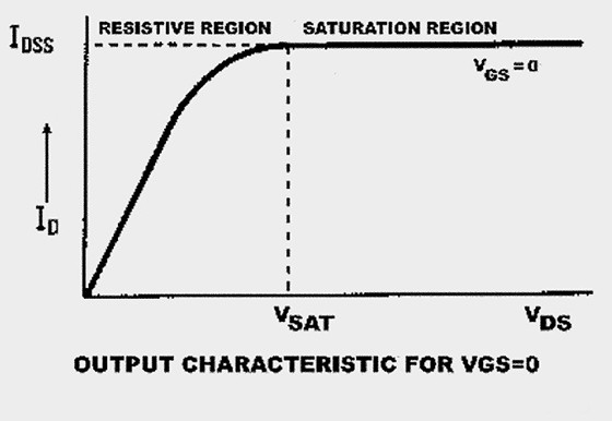
Depending on the doping of the semiconductor material, you get so-called Ntype or P-type material, and these result in the N-channel or P-channel types of JFET. The symbol for an N-channel JFET is shown in Fig. 1A. The three “electrodes” are called G, D, and S, for gate, drain, and source. The output characteristic for the N-channel JFET with the gate shorted to source (i.e., VGS = 0) is shown in Fig. 1B.
The characteristic field is divided into two regions, first a “resistive” region below the saturation voltage VSAT, where an increase in VDS results in a nearly linear increase in drain current ID. Above VSAT, an increase in VDS does not result in a further increase in ID, and the characteristic flattens out, indicating the “saturation” region. Sometimes these two regions are also called “triode” and “pentode” regions.
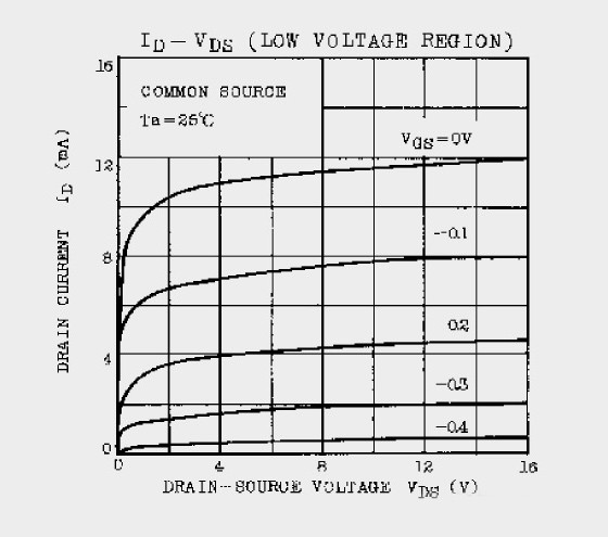
You can use the JFET as a voltage-controlled resistor or a low-level switch in the triode region, and as an amplifier in the pentode region. As you see, the Nchannel JFET conducts maximum current IDSS with VGS = 0V. If you apply a negative voltage to the gate, it reduces the current in the channel, and you get a family of output characteristics as shown in Fig. 2A. This device is called a “depletion” type of JFET.
In summary, the JFET consists of a channel of semiconducting material, along which a current can flow, and this f low is controlled by two voltages, VDS and VGS. When VDS is greater than VSAT, the current is controlled by VGS alone, and because the VGS is applied to a reverse-biased junction, the gate current is extremely small. In this respect, the Nchannel JFET is analogous to a vacuum tube pentode and, like a pentode, can be connected as an amplifier.
The P-channel JFETs behave in a similar manner, but with the direction of current flow and voltage polarities reversed. The P-channel JFET has no good analogy among vacuum tubes.
The Transconductance Curve
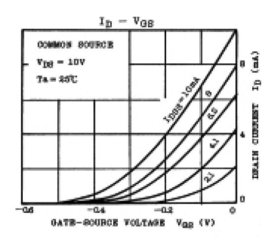
As mentioned previously, you can use the JFET as an amplifier in the pentode, or saturation, region. Here the VDS has little effect on the output characteristics, and the gate voltage controls the channel current ID. Because of this, it is easy to characterize the JFET in terms of the relationship between ID and VGS, that is, with the transconductance curve. Figure 2B shows the transconductance curves for a typical low-noise, high-gm JFET, the 2SK170.
The drain current as a function of VGS is given by the formula:

VP is the gate pinch-off voltage, and is defined as the gate-source voltage that reduces ID to a very low value, such as 0.1μA. The formula indicates that the transconductance curve has a square-law form. It also shows that if you know IDSS and VP, you can draw the transconductance curve for any JFET. The transconductance gm, which is the slope of the transconductance curve, is found by differentiating ID with respect to VGS:

The transconductance gm becomes −2IDSS/VP where the transconductance curve meets the y-axis. This is the value you normally find given in the data sheets. Notice that there are five different transconductance curves given for the 2SK170 in Fig. 2B. This indicates there is a range of ID curves for each JFET, due to manufacturing tolerances.
Also notice that the transconductance curve stops where it meets the y-axis. This is because the gate pn junction would be forward-biased if VGS were made positive for N-channel and negative for P-channel JFETs, and gate current would flow. This is analogous to the condition of vacuum tubes when the grid is made positive. Of course, a silicon pn junction does not conduct before the forward voltage reaches 0.6–0.7V, so you can apply several hundred mV in the forward direction without ill effects. JFETs are often operated with both polarities of gate voltage - i.e., with gate current - in RF applications.
The change in the transconductance curve is not just a matter of tolerances due to manufacturing, but it also depends on the temperature, and this is due to two different effects. As the temperature increases, the mobility of the charge carriers in the channel decreases, which leads to an increasing channel resistance, and hence a reduction in ID.
On the other hand, the barrier potential of the gate pn junction decreases about 2.2mV/°C, which causes the ID to increase. There is a point on the transconductance curve where these two effects cancel one another, and the temperature coefficient (tempco) becomes zero. Obviously, if you need to design for low drift, then the JFET must be operated at this point.
You can calculate the zero tempco point with the following formula:

Typical transconductance curves for two different JFETs are shown in Figs. 3A and 3B for a high-VP and a low-VP JFET, respectively.
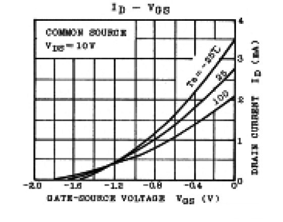
It is obvious from the curves that the zero tempco point occurs at a lower ID for high-VP JFETs and at a higher ID for low-VP JFETs. If the VP is close to 0.6V, then the zero tempco point is close to IDSS.
The Bias Point
As shown in Fig. 2B, the JFETs have a relatively wide range of transconductance curves. In order to operate the JFET as a linear amplifier, you need to have a clearly defined operating point. A typical common-source amplifier stage is shown in Fig. 4A. Assume that the +Vs is 36V, and you have selected a load resistor RL = 10k. What happens now if you insert a typical JFET, such as the 2SK170, for Q1?
Figure 4B shows five of the transconductance curves for the 2SK170, with IDSS between 2.1mA and 10mA. If you take one of these at random and operate it without RS, the actual drain current will be the IDSS value. With 2.1mA, the voltage drop across RL will be 21V; i.e., the drain (OUT) will be sitting at 36 − 21 = 15V. This might not be optimal from the point of view of maximum output or minimum THD, but it will work all right.
However, with IDSS = 10mA, the voltage drop should be 100V, which is clearly impossible with Vs = 36V, and the amplifier goes into saturation. Obviously, if you wish to use any or all of these JFETs, you must reduce the effect of the wide range of IDSS. The solution is to use a source resistor RS, similar to the biasing arrangements used in bipolar transistors or tube amplifiers.
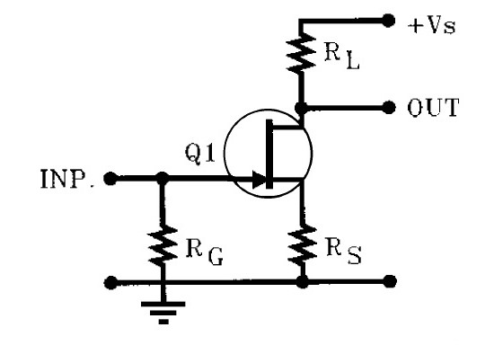
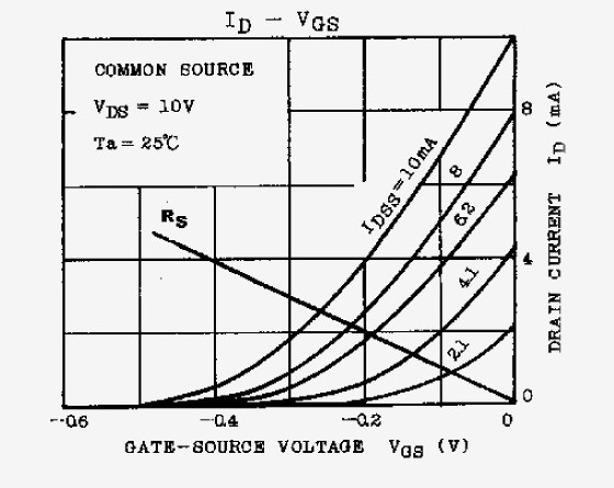
To illustrate the effect, I have drawn in the line for a 100Ω resistor in the transconductance characteristics. The range of drain currents is now limited between 1mA for the IDSS = 2.1mA device, and about 2.6mA for the IDSS = 10mA device. The drain voltages will be 36 − 10 = 26V and 36 − 26 = 10V, respectively. This is still too much variation from the point of view of THD and maximum output swing, but at least there is no saturation with any of these devices.
Fortunately, JFETs are sold with much narrower IDSS ranges, which makes life easier in terms of proper biasing. The 2SK170 comes in three IDSS groups: the “GR” group is 2.6–6.5mA, the “BL” group is 6–12mA, and the “V” group is 10–20mA. If you use a “GR” device with RS = 100Ω, the ID will vary between 1 and 2mA, which is almost acceptable.
The best solution, of course, is to select the devices for your particular application. Assume you wish to build a single-ended phono amp with JFETs and a passive RIAA correction network, and you decide to use the 2SK170 devices. In order to keep circuit noise to a minimum, you would use the 2SK170 without RS, i.e., at IDSS. Furthermore, you would need a relatively high current to be able to drive a passive RIAA correction network. If you choose, say, 5mA, you would need to select the devices from the “GR” group. But how? The selection is easy.
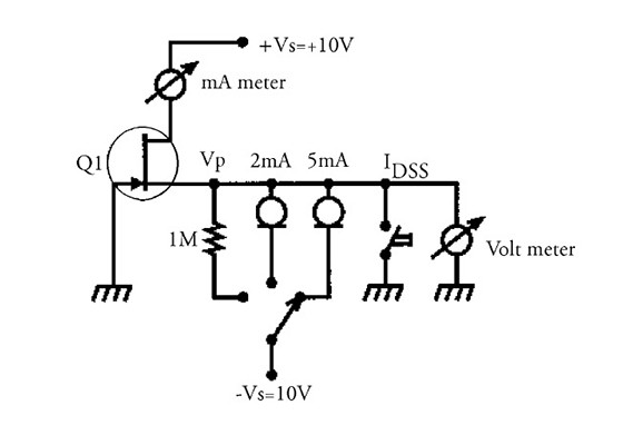
Testing JFETs
Figure 5 shows a simple circuit with which you can select JFETs and also match them if necessary. The tester feeds current into the source or connects the source to ground to measure the essential parameters of the device. In position 1 (switch in counterclockwise position), the source is connected to −10V through a 1M resistor. This feeds the source with approximately a 10μA current, which you can consider the cutoff point VP for the JFET. (Data sheets specify lower values, but this gives you a more practical value for measurements.) The voltmeter now indicates the pinch-off voltage VP for the device.
The next two positions measure the VGS for the device at given drain currents. These positions give practical readings for design purposes, and you can choose the constant-current sources for the values you need. The push-button switch shorts the source to ground, and the mA meter measures IDSS. If you wish to measure only VP and IDSS, you can permanently wire the source to −10V through the 1M resistor, which gives you VP, and then short the source to ground with the push-button to read IDSS.
If you test P-channel devices, you must reverse the supply voltages and the constant-current diodes. Normally, I test a large batch of devices (say 100 of each type) and sort them by IDSS. The different devices are then used in different applications.
Some Practical Measurements
As mentioned previously, the transconductance curve has a quadratic form, and if you wish to use it to amplify audio signals, it will create harmonics. A true quadratic curve would generate only second harmonics; however, ideal devices are hard to come by, and practical devices also generate some higher harmonics. Again, in this respect there is a close similarity to vacuum tubes. Looking at the transconductance curve, you can easily see that it is more linear close to the y-axis than further down on the curve. From the point of view of linearity, it is therefore an advantage to operate the JFET with a higher ID.
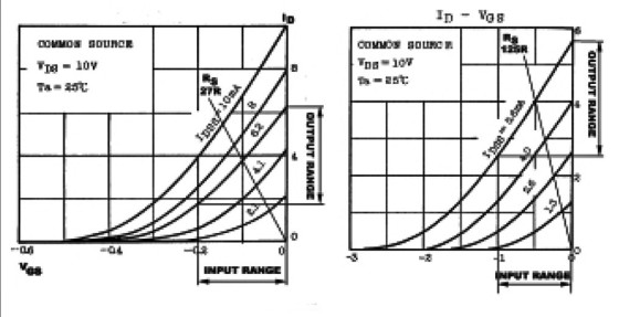
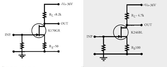
Figures 6A and 6B show the transconductance characteristics for two JFETs I use in many of my ampli fiers. The 2SK170 is a high-transconductance device with low VP, and the 2SK246 is a low-transconductance JFET with a higher VP.
I have selected a 2SK170 with IDSS = 6.2mA and a 2SK246 with IDSS = 5.6mA to illustrate the difference of operation with very similar values of IDSS. The gate pinch-off voltage is approximately 0.45V for the K170, and 2.75V for the K246. In order to operate them at the most linear part of the characteristic, I selected bias points at VGS = 0.1V and ID = 3.8mA for the K170, and VGS = 0.5V and ID = 4mA for the K246. These points are set with RS = 27Ω and 125Ω, respectively.
The most obvious difference between the two JFETs is in the maximum input swing with which you can drive them. The K170 allows approximately ±0.1V peak before the gate goes positive, but the K246 has a range of ±0.5V! Naturally, I could move the working point further down on the transconductance curve order to increase the input range, but eventually I would reach the other limiting point, where the gate cuts off at VP.
The thing to understand here is that a high-VP JFET has a wider range of input swing than one with a low VP. Other obvious differences involve the output range and the gain. With a ±0.1V gate voltage, the drain current varies between 1.8 and 6.2mA for the K170. With a drain resistor RL = 4.7k, this results in an output swing of 29.14V − 8.46V = 20.68V pk-pk. The gain will then be 20.68/0.2 = 103.4, which is 40dB. The output range for the K246 is 2.5mA to 5.6mA. With the same drain resistor of 4.7k, the output-voltage swing will be 26.32 − 11.75 = 14.57V pk-pk. The gain is 14.57/1 = 14.57 times, which is 23.38dB. That is, the high-VP device has lower gain than the low-VP one.
When Higher Is Lower
Of course, this can be explained by the transconductance. The gm for the K170 is 2IDSS/VP = 27.55mS. The gain is gm × RL, which gives 127 times, a bit higher than the graphical analysis. The explanation for this is that this gm is at the point where the curve crosses the y-axis, which is always higher than at the working point, and that the curve is not is not a straight line, making the output swing smaller than the theoretical value.
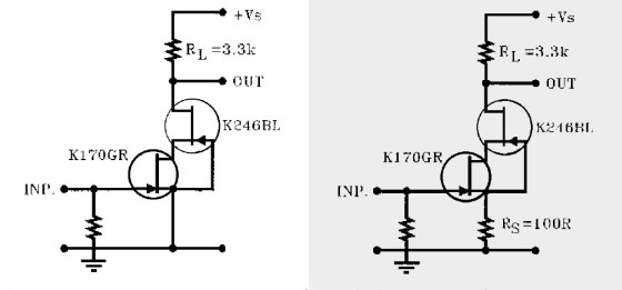
In any case, this quick calculation gives you a reasonable starting point from which to design the circuit. The corresponding gm for the K246 is 4mS, so obviously the gain is also much smaller at 19.14, that is, 25.63dB. Again, this results in a higher value than the graphical analysis. Now for some real circuits and THD measurements. Figures 7A and 7B show two amplifiers with K170 and K246. The K170GR had an IDSS of 5.5mA, and I operated it first with RS = 0 and RL = 3.3k.
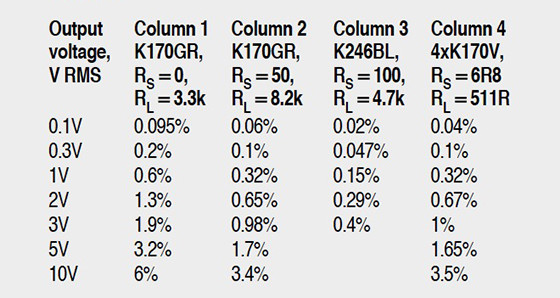
This gave me a gain of 36.4dB and a frequency response of over 400kHz. The THD is shown in Column 1 of Table 1.
Column 2 shows the same K170GR device, but this time with RS = 50Ω. This reduces the drain current to approximately 2.5mA, so I increased the drain resistor to 8.2k to have the same DC conditions as before. The THD is reduced by roughly 6dB. Column 3 shows the K246BL amp operating at ID = 5.1mA, with RS = 100Ω, and RL = 4.7k. The output is now a bit lower than half of the supply voltage, and the maximum output is therefore limited. But the THD is quite low, again about 6dB lower than the previous circuit.
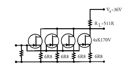
The K170GR circuit seems to be popular for phono input stages, and a number of these are circulating on the Internet. RS is usually shorted to achieve minimum noise. However, even without RS, the noise of a single K170 is not low enough for MC pickups. To achieve lower noise, you can parallel several of these devices. Doubling the JFETs with comparable gm reduces the noise by approximately 3dB.
I hooked up four K170s in parallel to see how it works (Fig. 8). Each device had an IDSS of approximately 15mA, and the drain currents with RS = 6R8 are 10mA each. With an RL = 511Ω, the drain is sitting at 14.8V DC. The gain is 34dB and the frequency response is 360kHz. The THD for this circuit is shown in Column 4 of Table 1. Remember that this circuit is working at very low levels, where THD is indeed low. The equivalent input noise is also reasonably low at approximately 100nV over a 20kHz bandwidth. Not bad for a simple circuit. Want to try it?
Input Capacitance
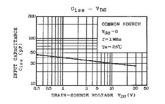
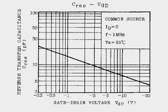
As mentioned before, the JFETs have a relatively high input capacitance, which can be an important design factor. Just like tubes and bipolar transistors, JFETs also have interelectrode capacitances that affect the frequency response of the JFET when it is used as an amplifier. The two capacitances, which are of importance for audio use, are the Ciss and Crss.
The Ciss is called the input capacitance and Crss the reverse transfer capacitance. Typical values for the Ciss are 30pF for the K170, and 9pF for the K246. The high-gm devices have a much higher input capacitance than the lowgm ones. The Crss is 6pF and 2.5pF, respectively. The Crss seems to be relative- ly low, but this is the one that dominates the input capacitance of an amplifier through the Miller-effect.
The input capacitance of a normal common-source JFET stage as shown in Fig. 7, but with RS = 0, is given by the formula: Cin = Ciss − Av × Crss, where Av is the voltage gain of the stage. Note that a common-source stage inverts the phase, so Av is negative, making Cin a positive number. Since Av can be a significantly large number, the input capacitance of the stage can be very high.
I have measured the input capacitance for the amplifier in Fig. 7, both with and without RS. Without RS, the capacitance was over 600pF! With RS = 100Ω, the input capacitance dropped to 127pF, because of the local feedback through RS. To appreciate the significance of this, assume that you are driving the amplifier from a 100kΩ volume control. The amplifier will see a maximum “source impedance” of 25k when the volume control is in the middle. If you calculate the 3dB point of the lowpass filter formed by the volume control and the input capacitance of 600pF, you find that it is about 10kHz! If you use the K170 without RS, you certainly must use a volume control, which is less than 100k.
Cascode to the Rescue
There is another way of reducing the input capacitance of the amplifier. Cascode connection of devices was invented in the tube era, but has also been used extensively with bipolar transistors. One of the advantages of cascoding, if you recall, is reduction of input capacitance, which makes it easier to design high-frequency amplifiers.
I have connected two circuits to test this (Fig. 9). The upper JFET needs a bias voltage, and it is easy to get this by connecting its gate to the source of the lower JFET. (Of course, you can also generate this bias from the supply voltage with a voltage divider, as you normally do with tube cascodes.) I am using a high-VP JFET for the upper device, so that the lower JFET has enough voltage across it to operate in the saturation region.
The input capacitance of the circuit in Fig. 9A is approximately 160pF, so the cascoding indeed reduces the input capacitance. Further reduction is achieved by adding local feedback with RS (Fig. 9B). The input capacitance is now reduced reduced to 50pF. With such low input capacitance there is no longer any danger of creating a low-pass filter with the volume control.
As though the existence and size of the input capacitance were not enough, it is also voltage dependent, which might cause distortion in certain applications. Figures 10A and 10B show the voltage dependence of Ciss and Crss, respectively, of the K170 JFET. Depending on the excursion of the input/output signal, you get a capacitance modulation, and this can cause distortion of the audio signal. This shows up mostly when you drive the circuit from a highsource impedance. I have tested the circuit described in Column 1 and Column 2 of Table 1 with different source impedances, and could not measure any significant increase in THD up to 50k source.
However, when the non-cascode circuit was driven from 500k, the THD increased approximately 6dB. The cascoded circuit showed no significant increase at any source impedance up to 500k. To avoid capacitance modulation problems, I recommend that you use a volume control of no more than 50k. (Of course, you would probably use no more than 50k anyway, because of the increased noise with higher impedances.) Note that in these circuits only two types of JFETs have been involved, whereas there are thousands of them on the market. Also, I have used them for illustration purposes only, and, although they work as described, I have made no attempt to optimize them for any particular application.
In Part 2 of this article, I will discuss the differential topologies.
Read also: "All-FET Line Amp” - published in audioXpress May 2002
Acknowledgements
My sincere thanks to Walt Jung of Analog Devices, who kindly read the manuscript and provided valuable comments and suggestions. Also thanks to our customers: Dr. Juergen Saile, Germany, Reza Habibi of Electro Concept Services, France, and Winfried Ebeling of Crystal Audio Research, Germany, for their valuable feedback, comments and suggestions throughout the ALL-FET development program.
This article was originally published in Audio Electronics, Vol 5 1999
Read more about the author here.