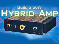
Design Approach
Your equipment should be designed to offer the best musical performance possible depending on costs and on the technology you are willing to use. It is often said that tubes sound better than transistors. I think this is not completely true, since the quality of sound does not depend only on the devices you are using, but more on how they are used. The approach when designing audio equipment is first of all to obtain the best electrical performance from the components you choose, and then to optimize the circuit for the best sound.
If you are not completely satisfied, abandon the first approach and look for a different design. Now, looking at a generic transformer-coupled tube power stage, you find that it has great handicaps: it is unable to supply large amounts of current to the load; its damping factor is very low; it phase-rotates in the low-frequency region; it is quite difficult to achieve an output power over 50–60W while still having good musical performance; finally, all of these and other parameters vary greatly depending on the regularity and nature of the load itself.
The list is long, but the greatest handicap is that tubes are unable to supply enough current to the load. This means that with some speakers you’ll never obtain good driving (and listening) performance from a tube amp. Now that the problem is clear, you can look for a solution. I am convinced that tubes do sound better than transistors, but the problem is how to achieve an exciting tube-sound driving performance from the power stage while avoiding the solid-state devices I need to use to affect the sound.
I can affirm that what makes good sound in an amp is mostly the first stage, the voltage amplifier. It adds gain, which means distortion, nonlinearity, and noise, but if carefully designed to operate with all the rest of the amp circuitry, it can really make a difference. The most suitable device to use here is a tube; I chose an SRPP design because of its low distortion, considerable gain, low output resistance, striking dynamics, and good slew rate.
The power stage is less critical; after all, it exists only to move current and drive the speakers. My choice here was a complementary solid-state-follower configuration, since it has no voltage gain and almost no distortion; it can move a great amount of current and deliver high peaks of it to the load; it has a very high damping factor and low output resistance; and, finally, it’s very reliable.
Now the question is: bipolar or MOSFET? Transistors are current driven. If you really wish to use them in your design, you need at least two current amplifiers to drive their bases, but this means more active devices that the precious signal must pass through, and this is not good for sound! Instead, MOSFETs are voltage driven, so you can derive the signal directly from the gain stage and apply it to their gates. Easy? Not at all! MOSFETs usually have huge source-to-gate and gate-to-drain capacitance, which means their gates will absorb current. The input stages must be able to supply this current; otherwise, frequency response and dynamics will be seriously compromised.
I have focused on the main points of the design: a tube gain stage, a tough driver, and a MOSFET power stage; and if what I’ve said is right, you’ll have an amp with superb driving performance that sounds very like tube equipment. The driver stage is AC-coupled to the power stage, which offers an enormous advantage in that you can choose the number of devices your power stage will contain without changing anything in either the driver stage or bias network, since MOSFETs are voltage driven.
Now you are dealing not just with a single amplifier, but with a complete amplification system that allows you an output power of from 50–200W. All ver sions will have the same timbre, the same sound, but different power, depending on how many devices you mount on the power stage.
This is exactly what I was looking for: an audiophile amplification system for my home-theater room. The 200W version powers the main speakers, and less powerful versions drive the other channels that are provided by a Dolby digital decoder.
Amplifier Design
One of my goals when I began to design this amp was not to use overall feedback; in other words, this needed to be an open-loop design. I think the only way to achieve a stable open-loop amplifier is to set a relatively low gain and let the preamp drive the power amp at full power.
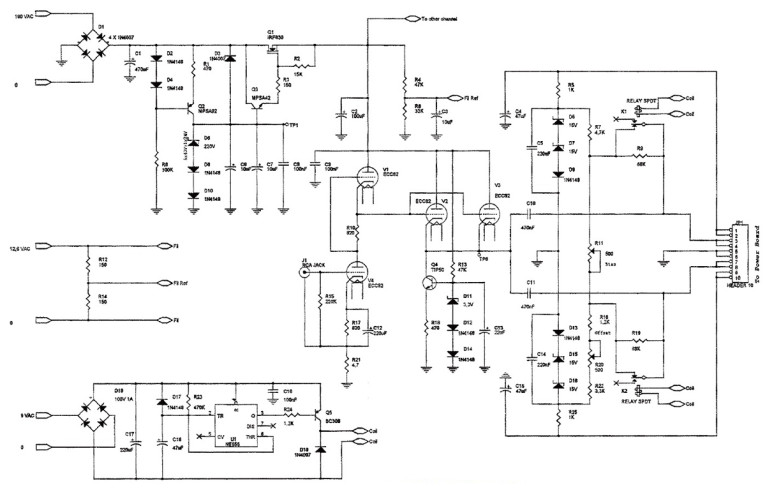
There is only one voltage amplifier here (Fig. 1). It’s a shunted regulated push-pull (SRPP) stage, which I think is the best solution, since it has a high gain and a good slew rate; it can deliver a large voltage swing, and it has low output resistance. It is based on an ECC82/12AU7, which sounds much better than the ECC83/12AX7 in an SRPP configuration and has a lower, but sufficient, gain.
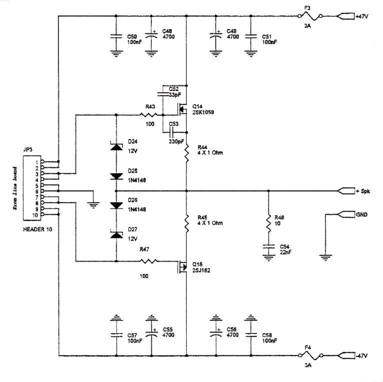
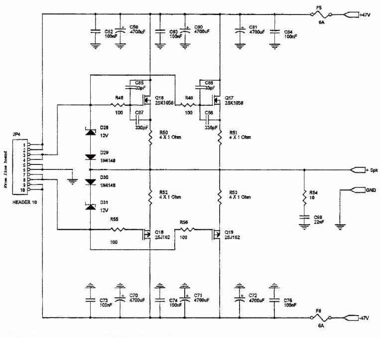
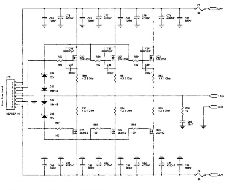
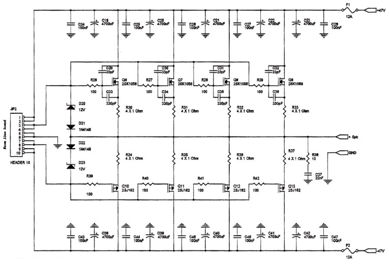
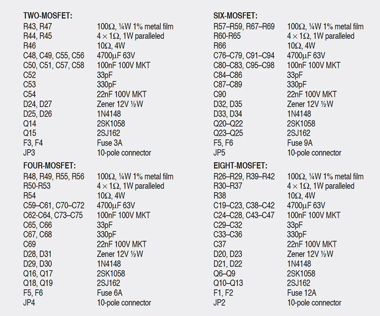
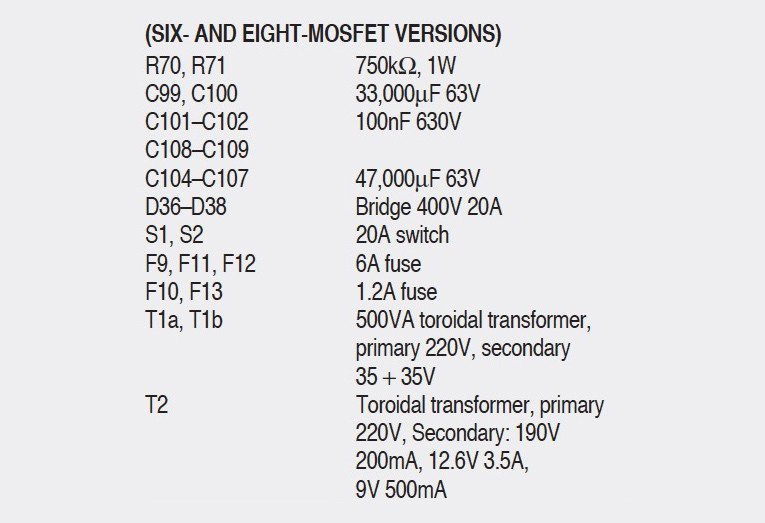
The power stage (Figs. 2–5) uses from two to eight complementary power MOSFETs in parallel. I have chosen the Hitachi 2SK1058 and 2SJ162 because of the great amount of current they can handle and for their S = 1 transconductance. I have already used these devices in a solid-state power amp, and was impressed by their reliability and very good musical performance.
It is true that the power stage is symmetrical like a tube push-pull, but it needs no phase splitter, since this power stage uses complementary devices. Notice that these power MOSFETs are used in a follower configuration (the N-channel loads the P-channel and vice versa). They therefore have no voltage gain, which means no added distortion and nonlinearity; they will only move current and supply it to the load.
Great Electrical Performance
The electrical performance of such a power stage is remarkable: almost no added distortion, a very high damping factor, a large amount of current delivered to the load, and extremely low output resistance. Now the question is how to drive it? It’s true that MOSFETs are voltage driven, but they have a considerably high source-to-gate and gate-to-drain capacitance, which means they do absorb current from the driver when a signal is applied to the gates.
Even if the SRPP has relatively low output resistance, it would not be able to drive four pairs of MOSFETs. Now imagine that all the input capacitance of eight devices is paralleled. This requires an extra driver stage, based on a tube so it can be directly coupled to the SRPP and loaded by a solid-state constant-current generator in order to enhance its performance. I paralleled two sections of an ECC82/12AU7 to increase the current flow and reduce the output resistance. The power stage is biased through a resistor network, where you will find two trimmers, one to set the bias current, and the other to correct and eliminate the DC offset.
What about the relay? During tube warm-up, the voltage on the driver’s cathode increases slowly until it is about half the supply voltage. Now this voltage is not constant, but variable, so it will pass through the coupling capacitors and the power stage will amplify it until the driver’s cathode is at its fixed potential. As a result, you have a huge DC voltage with almost no current limitation on your speakers. You can imagine what will happen.
During tube warm-up, the relay will short R9 and R19, connecting the gates directly to the biasing network, which has low resistance. In this way, the voltage swing on the driver’s cathodes passing through the coupling caps will be absorbed by the biasing network and will not drive the power stage. The speakers are safe now! This is how the amp works. Now let’s examine the reasons for some tricks you will probably notice while looking at the schematics.
Circuit Tricks
Consider the input plug. The negative lead is not grounded, but is connected to the R17/R21 node. R21 is not there to provide local feedback to the input stage since its value is too low, but it acts as a ground decoupler. I had some trouble with noise and hum, and this was the easiest way to make the amp mute. This trick, often used in preamplifiers and solid-state amps, is very simple and works well, but if your amp is still noisy due to a ground-loop caused by the input connections between the amp and preamp, try increasing R21 up to 15Ω. Bear in mind, however, that there may be other causes that make the amp noisy; in any case, check your layout first.
On the power boards, there are a couple of zeners, called “clippers,” between the gates and the speaker outputs that limit the current flow to 12A through each device, since a higher current might cause them to fail. I said before that MOSFETs have high interelectrode capacitance, but P devices have higher capacitance than do N devices, and since the power-stage design is electrically symmetrical, all N devices must be compensated. To do this, increase their internal capacitance with two capacitors mounted as close as possible to each MOSFET so they will all have identical capacitance. This will make the power stage more reliable by decreasing intermodulation distortion at high frequencies and increasing bandwidth.
On all the MOSFETs’ source pins, four 1Ω resistors are paralleled (on the schematics, only one resistor is shown). This is because power resistors have a little leakage inductance due to the way they are constructed (they are usually made of a wire wound on a ceramic base). The advantage of having four resistors paralleled is that you can use 1Ω carbon or metal-film resistors that have no leakage inductance, which is very important in maintaining a stable and reliable operation.
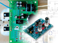
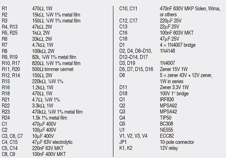
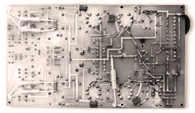
To make this amp work, you will need the driver board (Fig. 1) and one of the four proposed power stages (Figs. 2–5), which you just plug into the driver stage to enjoy your favorite music! The driver-board parts list is in Table 1, and the parts lists for the power stages are in Table 2.
Power Supplies
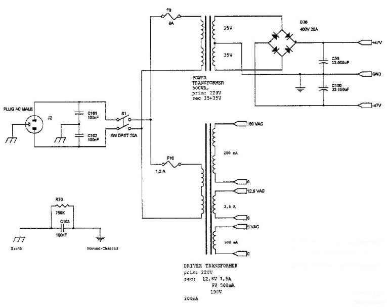
The input stage’s power supply is regulated; the circuit is the same as one I have used on the SV572-10 amplifier. A constant-current generator fixes a current through the zener series, and an npn transistor drives a power MOSFET used as a series regulator. This power supply, housed on the driver board, is the same for all versions.
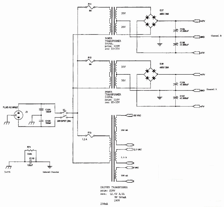
I mentioned before that this amp was designed to have a very high-performing power stage; as a consequence, its power supply must be very tough. Each version has its dedicated power supply (Figs. 6 and 7) giving current to the power stage. As you can see, these supplies are somewhat oversized because they must act as great energy reservoirs capable of delivering high peaks of current.
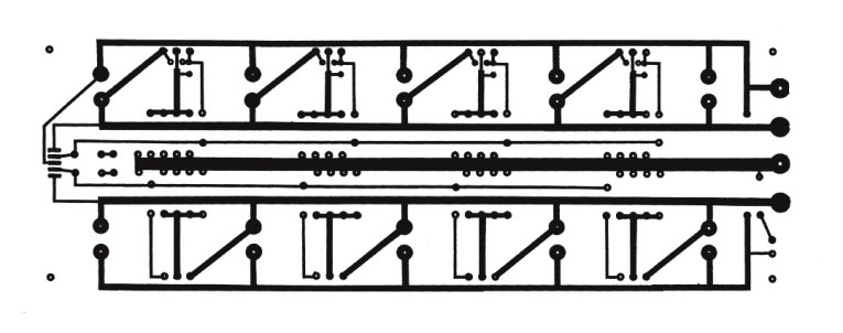
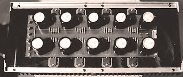
On the 8-MOSFET version of the power-stage board (Fig. 8), you will find ten capacitor cans mounted and paralleled five by five. This is still part of the power-supply design: five small capacitors paralleled have a lower Resr than an equivalent single capacitor, and finally, each power MOSFET is connected directly to the closest capacitor, allowing a very short connection between the power device and its power supply.
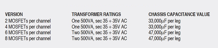
Unfortunately, having the filtering capacitance directly on the power board is very expensive. It also takes a lot of space, which necessitates having very long routes on the PCB — not a healthy situation. So additional capacitors are mounted on the amplifier’s chassis to allow you to reach the de-sired capacitance value. Refer to Table 4 for the appropriate values for each power-stage supply.
The 6 and 8 MOSFET versions have a double power-stage power supply, with separated transformers and filtering units for each channel, while all other versions have a common power supply for both channels. Finally, the driver board is supplied by its dedicated power transformer. Whatever version you choose to build will have a two-channel driver board with its power transformer and two power boards with their power supplies. Just plug one of the power stages into the driver board, and your amp will start working.
Mounting The Driver Board
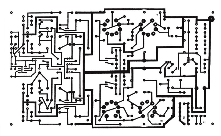
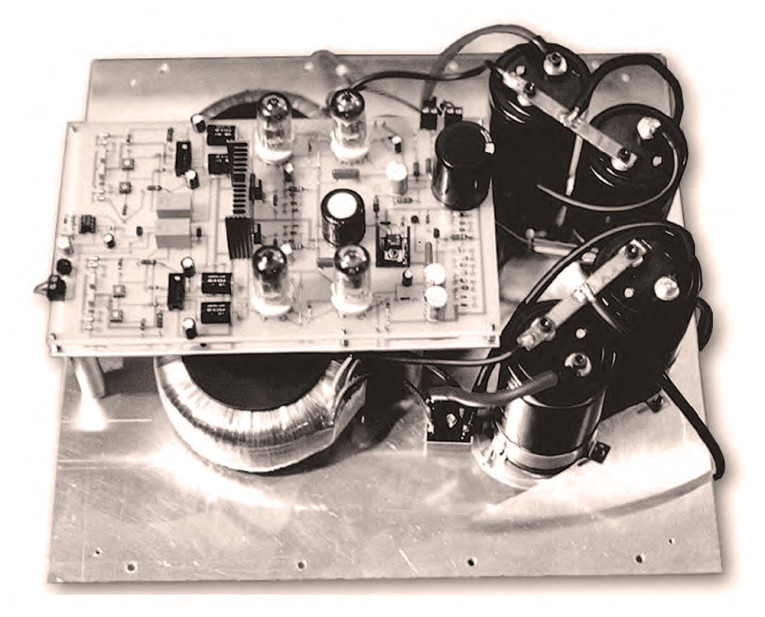
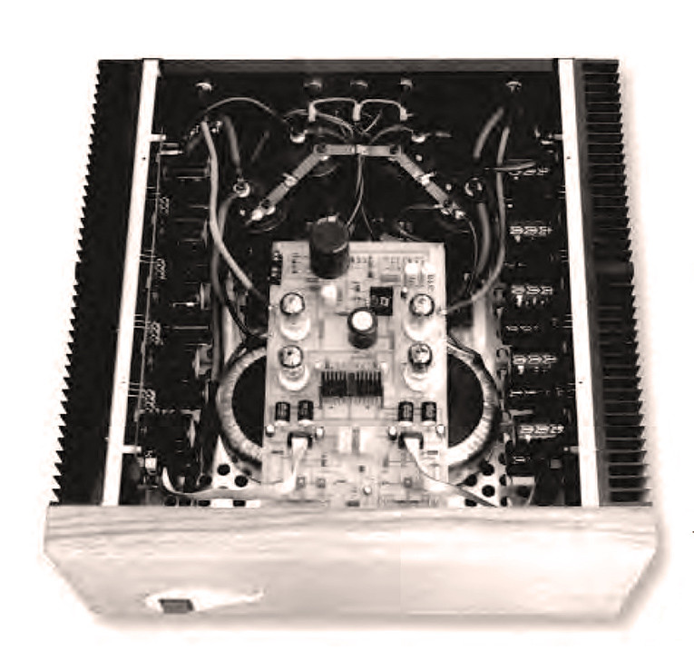
First of all you must make your PCB (Fig. 9, Photo 1) and have someone cut a 3mm-thick aluminum board with the PCB’s dimensions to shield the driver stage from the power transformers. In my layout, the power transformers are mounted just under the driver board, which I know is not the optimum solution, but I lacked enough space in my standard four-unit 19″ rack.
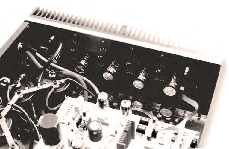
On the driver board, all connections between parts are routed except for the filament supply. Don’t forget that filaments are 12.6V operated, so you must connect the 12.6V to pins 5 and 6, leaving pin 9 unconnected on all tube sockets. Once you have your PCB finished, mount it on the aluminum board, leaving a 15–20mm space between them (Photo 2).
In order to reduce hum, connect a 100nF 400V capacitor between pin 9 of each tube socket and the aluminum board (Photo 3). The same must be done for each DC supply: the high-voltage drivers’ supply and both positive and negative legs of the power stage’s supply coming from the power boards to the 10-pin connectors you find on your driver board. All this is not strictly necessary, but it will help in reducing hum.
The driver-board layout (Fig. 9) is not updated with the ground decoupling network. You will need to cut the ground routes next to the inputs and solder R21 under the PCB. Next to the zener series there is a large ground connection that must be made directly to the power-stage power supply’s ground on the capacitors leads. This is the main ground connection between all power supplies.
Mounting The Power Boards
I have mounted and tested a prototype of each version, but I have finished only the most powerful one (8-MOSFET version), so everything I say from now on refers to this amp’s layout and construction. But don’t worry if you intend to build one of the smaller versions, because they all have many things in common, from the design to the final layout and construction.
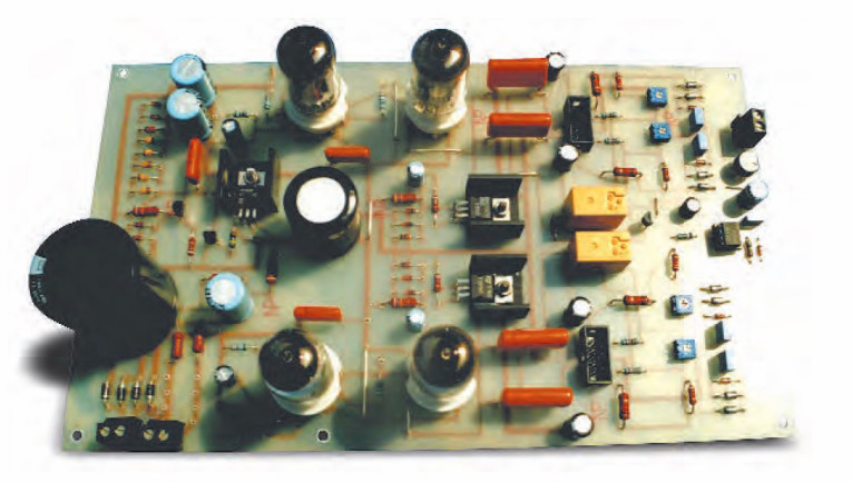
Mounting these boards won’t cause any trouble (Photo 4). By the way, pay attention when you mount the capacitors: the power supply has a positive and a negative lead with respect to the ground, so make certain the polarities of all electrolytic caps are correct. The positive lead supplies all the 2SK1058 MOSFETs, while the negative lead is connected to the 2SJ162 devices.
On the other side of the board, you may mount a 100nF 100V MKT capacitor under each 4700μF can; just solder each film cap directly to the 4700μF capacitor pins. There was not enough space on the component side of the PCB.
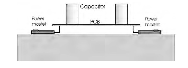
All MOSFET pins must be bent at 90° and soldered to the copper side of the board so that you can mount the power devices on the heatsink. Figure 10 and Photo 4 may explain much better than words how you do this job. Don’t forget that you must mount all MOSFETs on the heatsink with TO3P insulation kits.
Dissipating Heat
All solid-state devices produce much heat that must be dissipated. You will need a couple of large heatsinks. The best is one of those 19″ racks with heatsinks on its sides. A four-unit and 400mm-deep rack is required for the 8-MOSFET version (Photos 5 and 6). The 6- and 4-MOSFET versions will fit into three-unit racks, and I think the two-unit rack is sufficient for the smallest version of the system.
There are precise formulas and procedures for calculating the optimal heatsink dimensions according to the amount of power you must dissipate, but it would take too much space to describe all this. A little suggestion, however: when you mount a power device on a heatsink with its insulation kit, the rule of thumb is to be sure the heatsink is large enough so the running temperature never rises above 50–55°C. If you can still keep your hands on it without being burned, it means the temperature is 55°C, or less. But if the heatsink becomes too hot, you will need to mount a larger one.
Chassis Layout
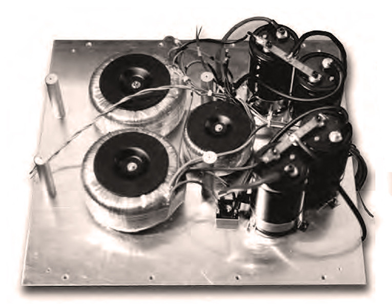
Once you have finished mounting the three boards, begin to think about the chassis layout. In my rack, the bottom board was not strong enough, so I replaced it with a 3mm-thick aluminum board. If you have the same problem, you will need to drill large holes in the board so that air may flow inside the box. As you can see from Photo 7, I mounted the three power transformers in the mid-front side of the chassis, the capacitor cans in the rear, and the bridges between them.
The driver board is elevated above the power transformers with four aluminum bars (Photo 2), and all secondaries of the driver-stage transformer are connected to the driver board. Both center taps of the two 500VA power transformers are wired to the main ground connection, which is directly on the capacitor leads. From there you must ground the chassis, the driver board, and both power PCBs. You must wire the positive and negative legs of the power-stage power supply from each bridge to the capacitor cans (watch out for the polarity!), and from the capacitors to the power boards.
The power-stage power supplies must be wired with 4mm wires. I have used 6mm wires, which you can do as well, but consider that they are not easy to solder. You will need a very big and powerful soldering iron. I made the ground connections between the capacitor cans with a 10 × 2mm copper bar, giving a very clean look to the layout (Photo 5). But, again, it’s really hard to solder a 6mm wire on it!
Don’t forget that the input plugs must be isolated from the chassis electrical ground. Finally, you will need a ten-wire flat cable to connect the power PCBs to the driver board.

First Start-Up And Tuning
Once you have finished mounting, check your layout carefully. Disconnect the power stage’s power supplies, turn the amp on, and be sure that the input stages do their job correctly (if you have a scope, use it!). Check the delay circuits 15 to 20 seconds after power is on.
The relay shorts R9 and R19. After a few seconds’ delay, the relay contact opens, unshorting R9 and R19. Turn the bias trimmer R11 until it shorts and the offset trimmer R20 half way. You must tune one channel at a time, so leave one of the two power supplies disconnected and connect a DC milliammeter in series with the positive leg of the power stage’s power supply of the channel you are currently tuning. Then connect to the output a DC voltmeter paralleled to a 10Ω resistor. Switch the amp on and turn the offset trimmer until you read 0V on your millivoltmeter; then set the proper bias current. Refer to Table 5 (the bias table) and look for the current required by the power stage you have built.
Wait until the heatsink has reached its running temperature and make the corrections needed to both bias current and offset. Be sure that the ammeter leads do not become disconnected while you are tuning the amp, or you will blow all the power devices! Repeat these few steps on the other channel, but before doing so, you must wait a couple of minutes until the capacitors are discharged; or you may discharge them yourself with a 1k 10W resistor connected between the positive and negative legs of the power supply.
Be very precise with the offset tuning. A 20–30mV offset is still permissible, but a 100–200mV voltage is not good for your speakers. Remember that all tunings on the power stage must be done with a 10Ω 10W resistor load connected to the outputs.
Measurements
At low levels, the THD is mainly due to the input stage, thanks to the power stage complementary follower configuration, which does not affect the signal in a significant way. THD increases at higher levels, since the power stage gradually switches from Class A to Class AB operation.
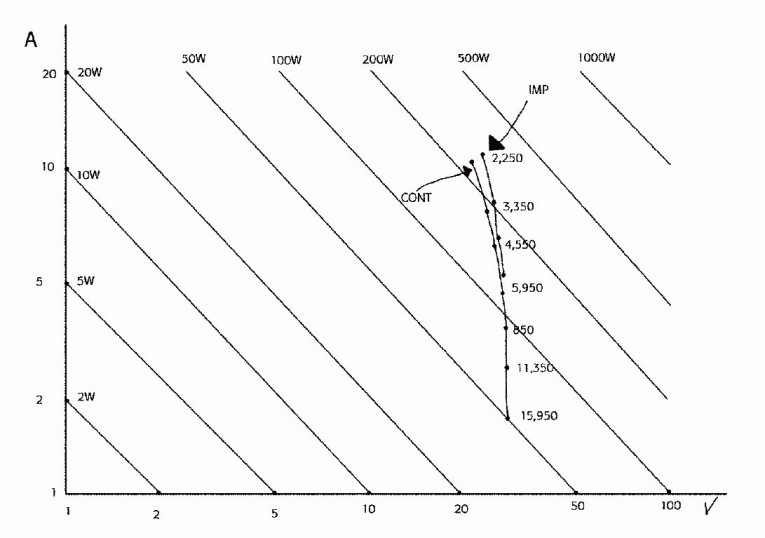
The graph in Fig. 11 reveals what the 8-MOSFET version is able to do, showing how the power stage reacts with different load impedances. The measurement has been done at full power (soft clipping) in both continuous and intermittent range (the test signal is a pulse signal). You may notice that it looks almost like a straight line, which indicates there is almost no voltage drop when a huge amount of current is required. As a result, you can see the benefits of the choices in both power-stage and power-supply design. Refer to Table 6 for further details.
Listening Impressions
I conducted all listening tests using the following equipment: a Pioneer PD507 CD player with custom output stage, a 6SN7 single-ended buffered by a cathode-follower preamplifier, and Magneplanar MG1.6 speakers.
In all versions, the timbre at low levels was substantially the same. What I said previously was correct: the input stage is the one that forms the sound of the amp. The timbre is very bright, but well balanced, with every detail clear. The high range is very precise, the bass is powerful and well damped, and the mid-frequencies are present and well linked with the upper and lower range.
Sometimes I sense that it is a bit rough in the midband, but less so than in push-pull tube amps. Consider, however, that I am currently influenced by the sound of the SV572-10 single-ended amp.
The virtual image is well focused. Voices and instruments are precisely defined and their images are very stable inside the virtual scene, giving a great sense of depth. The 2-MOSFET version has very good driving performance, but when high power is required, the image becomes a little confused. I think this is due to the fact that the power stage switches to Class AB at a relatively low output power.
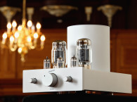
This does not happen with the 8-MOSFET version, since Class A is guaranteed up to 50W. The 200W version has extraordinary driving performances and damping factor. While mid and high-range performances are substantially identical for all versions, the 8-MOSFET-per channel amp (Photo 8) has an excellent bass response and striking dynamic range, allowing the best reproduction of every kind of music.
I love playing music with this amp at very low levels, because every instrument is so present and detailed, and the dynamic range is so wide, even when the speakers are just whispering. AX
This article was originally published in audioXpress, February 2001.
 About The Author
Marco Ferretti studied electronic engineering at the Turin Polytechnic in Italy. He became involved with tube amplification in high school, and then was attracted to audio reproduction. In the summer of 1994 he built his first power amplifier, a KT88 push-pull based on the famous Leak TL50. Since then, he has designed and built a number of amps, including single-ended designs.