Why is a regulated supply for (tube) circuits a good thing? If you look at a circuit, you see a DC source powering the stages. The implicit assumption is that the DC power source is just that— DC power, with no hum, noise, and ripple from the signal frequency. But that’s not the case, of course. There’s ripple and noise from the mains through the rectifier and smoothing circuits. Even if you get fancy with C-L-C and so on circuits, it’s never completely clean. And the load current that varies with signal frequency flows through the internal resistance of the supply, and Mr. Ohm showed us that current × resistance causes a signal-related voltage on the supply. Is that bad?
Every amplifier has a property called power supply rejection ratio (PSRR), which is a measure of how much of the ripple and hum on the supply bleeds through to the output. It varies with amplifier topology, of course, but it’s always there. Single-ended circuits are especially sensitive to this. So, a regulated supply that minimizes ripple, noise, and hum on the supply line is quite useful for clean, undistorted sound. Especially if it can be much better, smaller, and cheaper than a classic C-L-C circuit.
The Solution
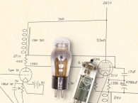
The idea for this project came to me when I was working on a broken 1970s Lambda 250V lab power supply. After spending a few hours on it, I found the problem: a defective voltage regulator IC, a 14-pin Lambda FBT-00031. Tech support at Lambda kindly provided a single spec sheet for the chip. It took several weeks for someone on the Internet to identify the chip as a re-branded Motorola MC1466L (Fig. 1), which was obsolete, of course.
I found two NOS sources: one in the Far East to the tune of $280 each for a minimum order of four, the other in nearby Germany for 6 euros each. I ordered a couple, replaced the chip, and the supply worked perfectly. I found the conceptual approach of this chip, with a floating error amp and reference setting with a single resistor, so intriguing that I decided to see whether I could apply it to a high-voltage tube regulator.
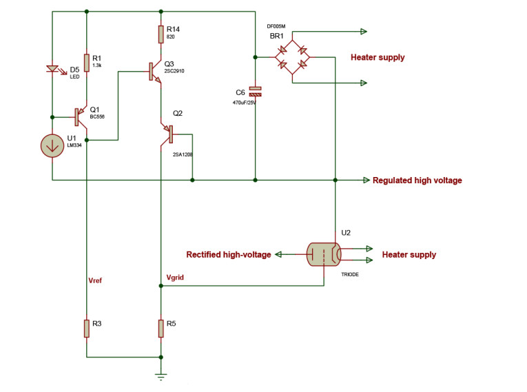
The concept of my circuit is shown in Fig. 2. This is a high-voltage regulator, but I’d like to avoid as much as possible relatively rare and expensive high-voltage devices and parts. That’s why there is a separate low-voltage supply, floating on top of the high-voltage output. This low-voltage supply, powered from the rectified pass tube heater, runs the reference and control circuits, which can be low-voltage.
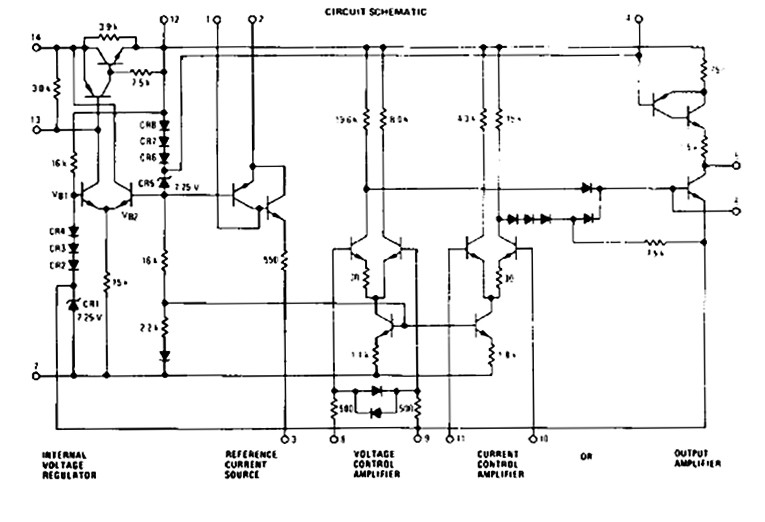
This type of regulator consists of the same modules. There is always a reference voltage and an error amplifier that compares the reference voltage to (a sample of) the output voltage. The error amplifier then drives the pass element to control the output.
How It Works
In my circuit, the reference voltage comes from resistor R3, driven from the floating constant-current source Q1. Q2 and Q3 form the error amplifier. It is a differential amplifier, but with complementary devices rather than the more usual difference amp with two similar devices. But it works the same: the reference is input at Q3, and regulated the output voltage is input at Q2.
If the output voltage falls below the set value, Q2 will start to conduct more, and the drive voltage for the pass device across R5 will increase, which, in turn, increases the output until it is again at the set value. Similarly, when Vout becomes too high, the drive is reduced, lowering Vout back to the set value. Because Vout is equal to Vref except for a 2-Vbe offset, in principle you can set the output voltage to anything you want by just selecting R3. This is a great advantage to more traditional setups.
Traditionally, you would have a reference voltage that is some fraction of Vout, and then you divide Vout down to Vref before feeding it into the error amplifier. If you want to change Vout, you must change the division ratio. The disadvantage is that this also changes the loop gain of the control loop, which again means that the performance and stability change with output voltage. By using a reference voltage equal to Vout, as I have done, the stability and performance of the circuit does not change with output voltage.
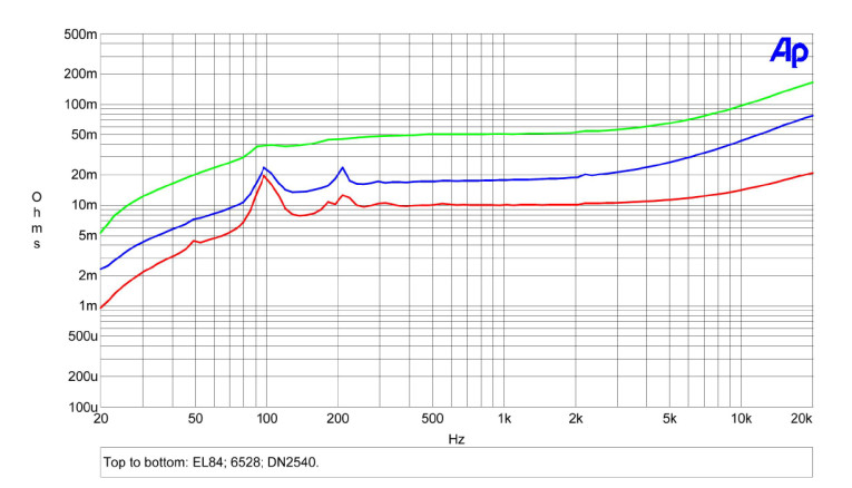
You may wonder why the error amplifier is such a simple circuit. Certainly, using a high performance op amp here increases performance, but not enormously. And such op amp-based very high gain circuits bring their own issues with stability and compensation, for instance. In fact, the circuit as-is is already pretty high performance, as shown in Figs. 3 and 4.
One reason for the good performance is that the load resistor for the error amp is the resistor from Vdrive to ground, R5. Using a tube as a pass device, this resistor forms the grid resistor, which should be around 500kΩ, depending on the device. So, even a very small error between B and E of Q2 will lead to a relatively quite large “correction” current through R5, and thus to a quite large correction voltage at Vdrive. This loop gain is pretty large notwithstanding the simple circuit, so I decided not to use a high-gain op amp.
Other Considerations
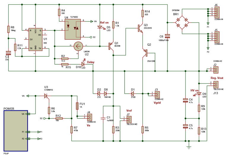
This being a tube regulator, there are a few other factors to consider. One is the delayed application of the anode voltage, not just for the pass device, but also for the amp to be supplied. The full circuit (without the pass device) is shown in Fig. 5. U1 is a standard 555 (CMOS) timer that pulls down the LED in U4 some time after you switch on the supply.
The delay is set by R8 and C3, and with the given values is about 30 seconds. You can shorten it by lowering the value of C3, or make it longer by increasing R8. Depending on the leakage of C3, 1MΩ is probably the maximum value for R8. Once the LED in U4 is on, the opto-triac will fire and switch on thyristor U3, which will apply the rectified high-voltage to the pass tube (J4). Because the pass tube needs a heater voltage, I used that also to power the reference and control circuits through rectifier BR1 and capacitor C6.
An important factor is the “cleanliness” of the reference voltage. If there is any hum or noise on the reference, it will be faithfully duplicated by the error amp on the output. Current source Q1 gets its reference Vbe through the LED D5. With R1 being 1.3kΩ, the reference current is almost exactly 1mA, which makes the selection of the reference resistor R3 easy: just 1kΩ for every volt output you want.
LED D5 acts as a voltage source and is pretty clean. However, the first prototype did not have current regulator U2, but just a resistor to set the LED current. The hum on the control supply caused hum across the LED biasing resistor, which caused very small hum across the LED, but enough to appear in the reference. I also noticed that the output voltage decreased several 100mV with load changes of 100mA. The reason: both the high-voltage supply and the heater supply came from the same transformer.
Increasing the load made the transformer secondary voltage drop slightly, including the heater supply that supplied the reference and control circuit. This was enough to slightly lower the current through the LED, and therefore the reference voltage. In other words, increasing the load lowered the reference! I then tried a voltage regulator for the reference and control supply. That worked, but I lost some flexibility with the heater voltages because a (5V) regulator also needs some dropout reserve.
Finally, I settled for the current regulator U2, an LM344, which performed even slightly better than a voltage regulator on the supply. There are some other parts on the schematic for protection purposes. The most obvious one is the fuse FU1 in series with the high voltage. Next there’s protection for the transistors. For example, if the high voltage is switched on by U3, the reference voltage at the collector of Q1 needs time to rise up by charging C1. During that time, transients on the output line could be much higher than the safe value Vce for Q1. D2/D8 limits this value.
Protection for Q2 is also required for the same reasons: under transient conditions, Vout may peak above the required value. Q2 will try to correct that which may cause the Vc of Q2 to drop momentarily to a very low value. Vce of Q2 is limited to 100V by D1. This means that Vgrid can be maximum 100V negative with respect to Vout, the pass tube’s cathode voltage. This value should be sufficient even with low-mu triodes and low load current. R14 limits the maximum current through the small-signal transistors during startup and transient conditions.
Configurations
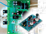
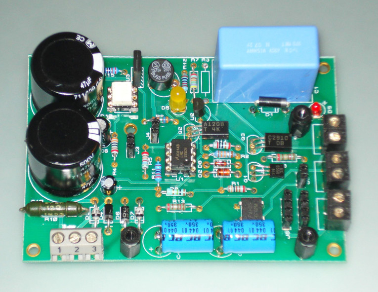
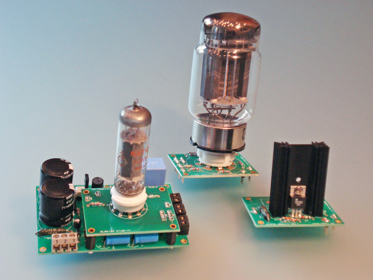
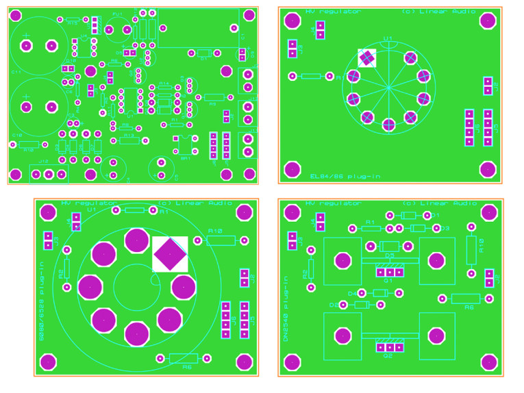
Because this supply is pretty universal as to the output voltage (in principle from the minimum Vgk of the pass tube up to 500V, limited by the voltage rating of the high-voltage rectifier and capacitors), I thought I’d also make it flexible as to the current it can supply. The rectifier, reference, and control circuits fit on a “motherboard” type of PC board (Photo 1). Then there is a small plug-in-board that carries the pass device and some resistors, and that is plugged into the motherboard.
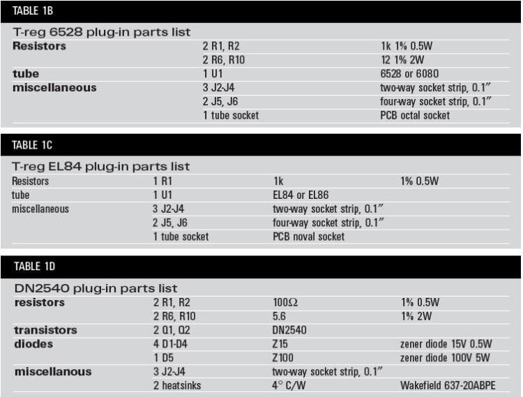
This way, you can use the regulator with different pass devices depending on your load current. Currently, I have three plug-in-boards (Photo 2). For power amps, the plugin-board with a 6528 dual triode tube can deliver up to 600mA (with a suitable power transformer, of course). This tube is specifically developed for series regulation. A 6080 tube also fits on this plug-in board. Due to its lower mu, it has a slightly higher Zout and slightly higher hum and noise, but if you happen to have one of those lying around you can use it with good results. The plug-in fitted in the photo is a board with an EL84/EL86-type triode-connected small pentode for preamps and similar loads, up to 50mA.
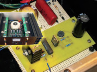
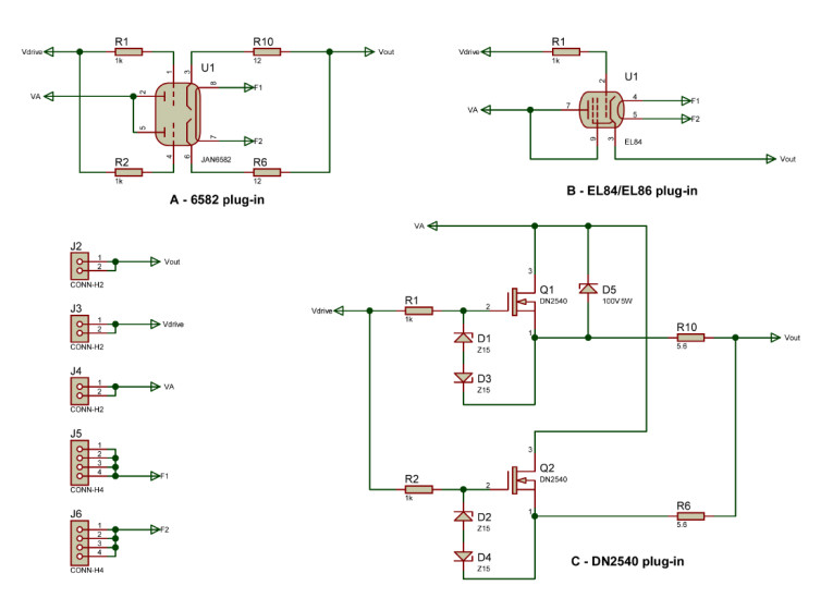
Last, for those who want a “green” version and save 10W or so on the pass tube heater, there is a board with a depletion mode MOSFET, a DN2540. This particular plug-in-board can accommodate two DN2540s and their heatsinks for an output load of more than 1A, depending on the dissipation from the Vds drop. The circuits for the plug-in-boards are shown in Fig. 6. Because the 6528 (6080) are dual triodes, there are small value cathode resistors to equalize the currents at higher loads. The same is used on the DN2540 board in case you use two devices for increased load capacity (you can short the source resistor if you use only a single DN2540).
The plug-in-boards also have grid and gate stoppers for added stability. The DN2540 board has an additional 100V/5W zener diode (D5) to protect the MOSFET during switch-on and load transients as well as Vgs protection zener diodes. It also accepts a pair of standard heatsinks; tubes are definitely at an advantage in the dissipation department.
The boards are connected with standard 0.1″ pitch PCB connectors and headers cut to size. Note that when you use the MOSFET pass device you don’t need the heater connectors between the two boards. M3 machine screws and 12mm standoffs secure the plug-in to the motherboard.
Performance
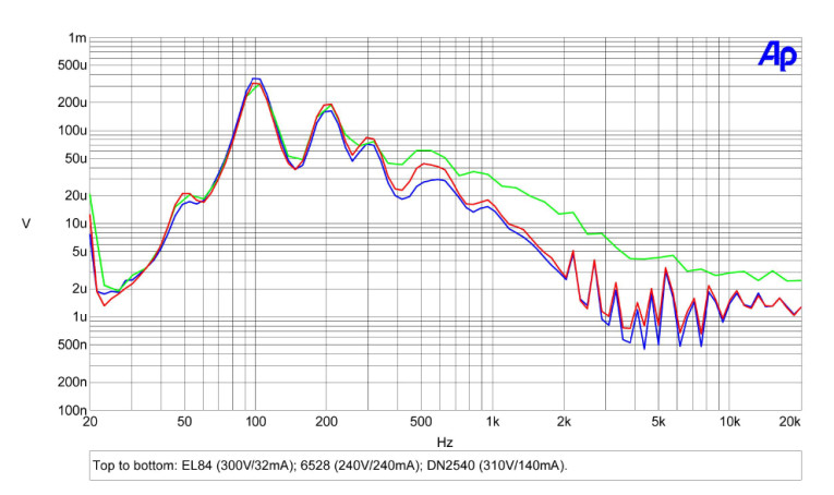
Figures 3 and 4 show the output impedance and output hum and noise of the various versions over the audio band. The performance is quite respectable for a high-voltage tube supply. The best all round performer is the MOSFET, because of its high transconductance; however, differences are small. Hum and noise under load are typically below 500μV RMS in a 20kHz bandwidth for all versions (mostly line-related hum components).
You may wonder why I actually built three versions. Why not just use the DN2540? It is the best performer, and it has another advantage: a lower dropout voltage. The DN2540 works fine with just 10 or 15V Vds (depending on the input ripple), while the tube versions require several tens of volts Vak to operate cleanly. This means that for a given transformer the DN2540 provides 10 to 15V more DC output and less dissipation. But there’s more to it than just measurements. Although I would be hard-pressed to hear any difference between those regulators powering an amp, there’s always the “X-factor.” You may prefer a tube regulator in a tube amplifier for perfectly good reasons. So, the choice is yours!
Customization
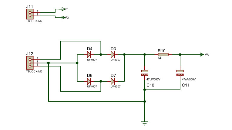
The input voltage is limited by the voltage rating of the rectifier diodes and capacitors — 500V peak in my version. That limits Vout to about 485V with the DN2540. If you need more output voltage, you can use higher-rated diodes for D3, 4, 6, 7, and C10, 11 (Fig. 7). Note that the diodes should be rated for at least twice the rectified peak voltage, preferably more. It is always wise to keep a healthy margin for the diode and capacitor ratings to cope with unloaded output voltages and high mains levels.
You can use a transformer with a single secondary connected to J12 pin 1 and 3, or a center-tapped secondary with the tap at J12 pin 2. In the latter case you can omit diodes D4 and D6, of course. The board has provisions for a small resistor between the two reservoir capacitors (R10) to take the high-frequency edge off the ripple voltage. The 12Ω is probably a bit too high for load currents above 100mA, so you should experiment with it, or short it out altogether. You can also use off-board reservoir capacitors and/or chokes. Lowering the ripple on the rectified voltage will not, however, bring a 1:1 improvement on Vout because the ripple on Vref will start to dominate.
As-is, the performance is pretty well balanced. As noted, the output voltage is 1.2V below Vref. You can easily set Vref by selecting R3. With the reference current approximately 1mA, Vref (in volts) = R3 (in kΩ). Note that you can use an external resistor or pot meter at J7 to set Vout. If you use a pot, be sure to use one that can withstand 500V! Provided that you have enough rectified input voltage, you can set Vout to any value within reason. The minimum Vout depends on the negative grid/gate drive voltage. If you make Vref = 0 by shorting R3, the DN2540 gets pretty close to zero as well, but a 6528 will not go lower than tens of volts (depending on the load) because of the necessary negative grid bias. The output at the cathode will need to be above the drive voltage at the grid, except for quite high output currents.
Construction
Before starting construction, note that this supply contains points with lethal voltages and currents, including the heatsinks for the DN2540s! You are responsible for your own safety, not me, nor the folks at aX. Double-check that the high-voltage input is disconnected or turned off before working on the board. Discharge the high-voltage capacitors with a 1k resistor. Make it a practice to keep one hand in your pocket when touching live boards with a meter probe or anything at all to avoid body currents. Even when switched off, the high-voltage capacitors may still have a dangerous charge. Discharge them.
Warning: the heater supply for the pass tube is also used for the reference and control circuits, and floats on the regulated high-voltage. Do not use this heater winding for any other tubes in the equipment to be powered. If you use the DN2540 plug-in board, you still need a separate floating supply for the reference and control circuits. In any case, you could also use a small separate 5 or 6V AC transformer, provided it has enough secondary insulation to allow it to float to up to the maximum Vout. Construction is straightforward when using the motherboard-plug-in board approach. Figure 8 shows the component stuffing guides for the motherboard and the plug-ins. The complete parts lists are in Tables 1A-1D.
It is best to start with the small parts on the motherboard, such as resistors, diodes, transistors, and headers, leaving the larger caps for last. Take care to mount the pins and headers straight upright. The hole locations on the plug-in boards correspond exactly to those on the motherboard, but if the pins and headers are slightly off vertically, they mate less smoothly. The transistors are below the plug-in board. Because of the height limitation, you should fold them horizontally on the board as shown. Do the same with the output electrolytics C4 and C5. The layout has open space for that.
You can test the motherboard without plugging it in, to verify that the delay and thyristor circuits work. LED D10 should light when switched on, while D5 should come on after the delay time. (D9 will not come on unless you have a pass device plugged in.) The input voltage at J4 should also come on after the delay. Next, populate one of the plug-in boards, mount it on the motherboard, and check out the whole assembly. Well, that’s it.
I’d appreciate some feedback about your experiences with this supply. You can contact me via my website www.linearaudio.nl. I will also post any additions and tips there. Happy building and happy listening!

Postscript
After completing the prototype, I received an e-mail copy of the June 2008 issue of LT Magazine, which featured the new LT3080 Linear Regulator (Fig. 9) that looks conceptually exactly like an MC1466L that was declared obsolete more than a decade ago. What’s more, this chip was selected by EDN as Innovation of the Year, while LT’s Chief Technical Officer Bob Dobkin was named Innovator of the Year. I guess you should be very careful about what you declare obsolete. AX

This article was originally published in audioXpress, April 2009.