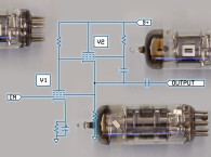
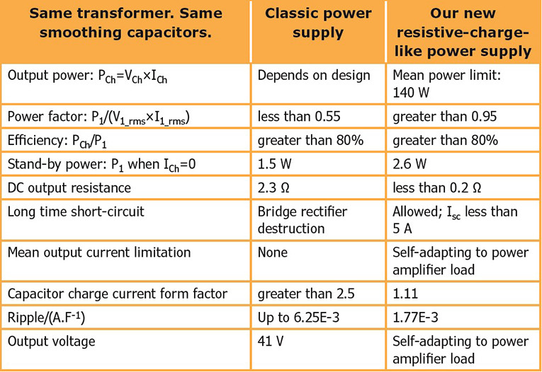
This project introduces an improved design of a power supply for audio amplifiers (see Photo 1) that behaves like a resistive load with respect to the mains network. Thus, the current drawn from the mains has the same shape as the voltage delivered by the mains and has the same phase, so that the power factor is very close to 1. Consequently the RMS value of the current drawn is as low as possible and that offers several audio benefits.
For this project, I was careful to limit building difficulties. What you get from this power supply is good power rail regulation and low power rail ripple with low harmonics. You also get lower 50/60 Hz electromagnetic pollution. A comparison of the classic and new approach is shown in Table 1.
The power supply is dimensioned for 100 W RMS/4 or 8 Ω power amplifiers. Thus, the output power is simultaneously limited by the regulation of output voltage and the output current. This article focuses on a practical realization of the power supply. The design, development, technical, and theoretical background is explained in a more extensive article in Jan Didden’s Linear Audio Volume 12. That article is now also available online here.
Since the RMS current is low and almost sinusoidal, the transformer doesn’t have to be over-dimensioned. Second, the electromagnetic radiation from the supply and the transformer, which often cause disturbances to the power amplifier, is lower and has less harmonics. Third, you won’t have to buy an expensive shielded mains cable.
Because the output is regulated, the DC output resistance is low. This is important when you want to get extended full power from the power amplifier. The classical solution would be to over-specify all the power supply components. Transient response is also both faster and has lower ripple. Because the form factor of the current IR charging the smoothing capacitors is close to 1, these capacitors can be up to four times smaller.
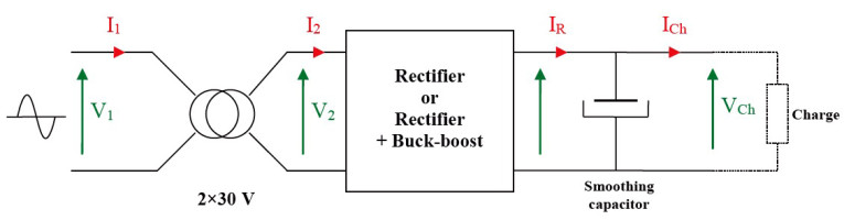
Now suppose you are building a power amplifier. The classic solution for the power supply is to use a transformer, a bridge rectifier, and smoothing capacitors.
Suppose this is a 100 W RMS/8 Ω power amplifier. To correctly rate your power supply, you need to take into account:
• The power amplifier’s quiescent current
• The loss of voltage across the power transistors
• The efficiency of Class AB power amplifiers at full power
• The power supply’s DC resistance
• The power supply’s power factor
• The transformer’s efficiency
You may need at least a 300 VA (600 VA for stereo) transformer. That’s why DIYers often use “overdimensioned” transformers and they are right to do so. You will also want to keep the DC resistance as low as possible to get full power out of your amplifier. You will want the power rails ripple to be as low as possible, since your amplifier’s limited power rail rejection ratio could lead to power amplifier hum. The “classic” solution is to use huge power supply capacitors.
With this new power supply, you won’t have to over-specify the transformer because of the excellent power factor, correct performance, and output regulation—150 VA is enough. You also won’t have to over-specify the smoothing capacitors because of the current feeding these capacitors.
Finally, your listening experience will improve at low levels and high levels. (Note that the output ripple is also important when the power amplifier saturates. Smoother ripple will give less unpleasant distortion.) Mid-level listening experience probably won’t change much, except maybe through the satisfaction of using a more ecological power amplifier.
It is widely acknowledged that power consumption is an ecological issue but so is avoiding drawing reactive and distorted currents. Fortunately, these issues can be highly compatible with audio enthusiasts’ wishes. That’s why I propose this DIY power supply.
The Power Supply’s Topology
This kind of power supply is not revolutionary. Its design has existed for may years, but unfortunately it is not used for power amps. And while this project would work even without a transformer, I have integrated a transformer into this design for one major reason: A transformer-less power supply can be dangerous to work on, so I prefer it to be safe from high voltage areas. The fact that it can be a small transformer, combined with the relatively low value smoothing capacitors, compensates for the cost of the circuit board, so it remains an economically viable solution.
The topology is not the most popular one, which combines a switching power supply preceded by a Power Factor Corrector (PFC). The method employed here is called the “Imax method” (see Figure 1). The main difference is that it only employs a single structure. You can find one or more ICs dedicated to this topology but I don’t use them for two reasons.
First, I try not to use specialized chips for my DIY projects so the components can be easily sourced. Second, these specialized chips switch at constant frequency and that does not suit a variable output voltage design because of a natural switching between two modes, which causes the current to no longer be sinusoidal. Finally, eliminating specialized components offers more flexibility and scope for further evolution, and you can learn more by studying the project.
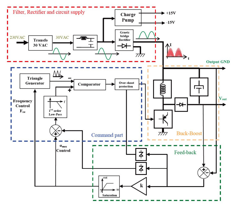
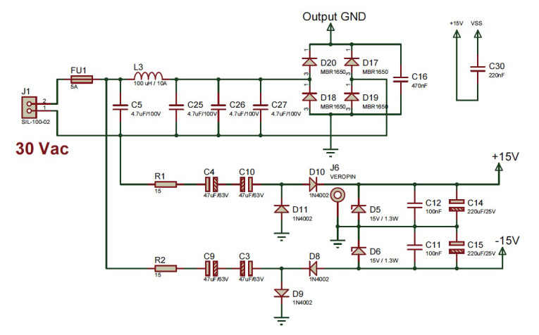
So, basically, the heart of the power supply is a buck-boost structure. It always works in full demagnetization mode so that IMAX (peak current into the coil) is proportional to Ton and to the power rail voltage of the switching structure, which is the transformer’s filter and rectified output. Thus, the current drawn from the transformer is shaped the same as the mains voltage and its amplitude is proportional to Ton. Figure 2 shows a functional diagram of the power supply’s filter, rectifier, and circuit supply.
Ton is controlled via feedback to regulate the output voltage, whatever the output current IC is. Ton limiting provides a current limit that causes power limiting (by saturation of the feedback) when the output voltage Vout is greater than 33 V. When the power supply is short circuited, the coil becomes noisy because of the low switching frequency but the current never exceeds 6 A and is even lower when Vout is shorted to absolute 0 V.
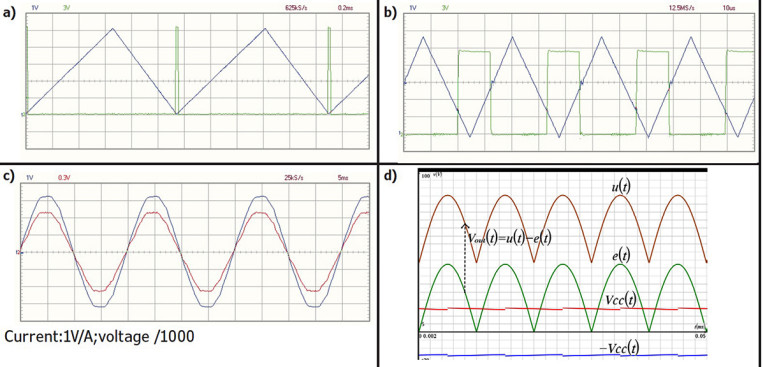
I will not go into further circuit details here. However, more detailed math and theoretical explanations for this project will be available in my article included in Linear Audio Volume 12. Here we will focus on the practical application. Table 2 shows the power supply waveforms.
Circuit Elements
The circuit elements include the LC filter, the rectifier, and the charge pump; the buck-boost structure; a triangle generator; nonlinear feedback; linear feedback; and a power MOSFET driver. The LC filter smooths the current drawn by the switching converter and then provides the mean of this current during a switching period before the filter (see Figure 3). For the rectifier, the mean current in a switching period is a rectified sine after this rectifier (always positive), and is sinusoidal before it. The diodes are Schottky diodes, which are mounted on an angle bracket for heatsinking. The charge pump supplies the auxiliary voltages for the regulation circuit.
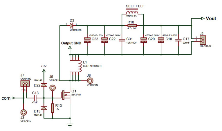
Figure 4 shows the buck-boost structure. It may seem to be a boost structure, but it is working as a buck-boost because the output ground is not the structure’s ground but the structure’s supply rail. I made the coil. A YouTube video on its construction can be found on my website (www.muselec.fr). It’s easy enough to wind it yourself. You need 4 m of cable made of more than 600 wires. The many strands ensure that the skin effect will be low. This is critical for these applications because of the high and fast-slewing current variations into the coil, due to the complete demagnetization mode. Choose low ESR capacitors (C22, C23) to get better efficiency and longer life expectancy. They must not be lower in value for stability reasons, but they can be larger.
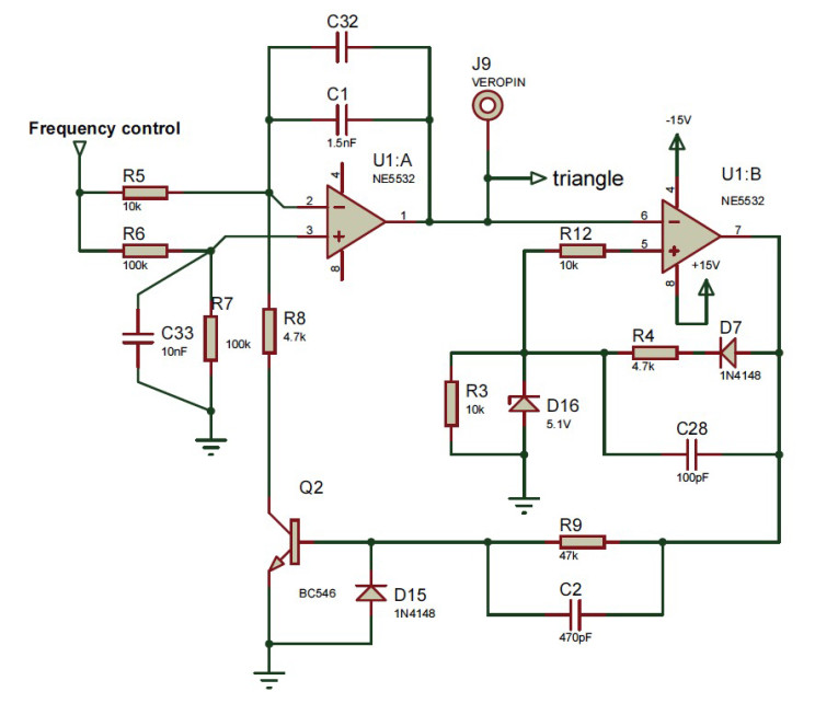
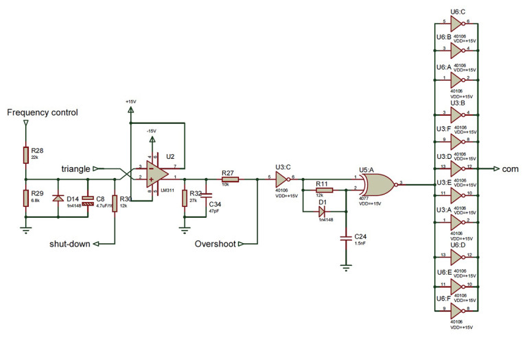
The triangle generator’s frequency is controlled by the feedback input. The output of this generator is compared to the feedback voltage to drive the MOSFET (see Figure 5). Since the feedback controls the frequency of this triangle generator and the switching Ton/Tsw at the same time, as the frequency varies, Ton_max is unchanged.
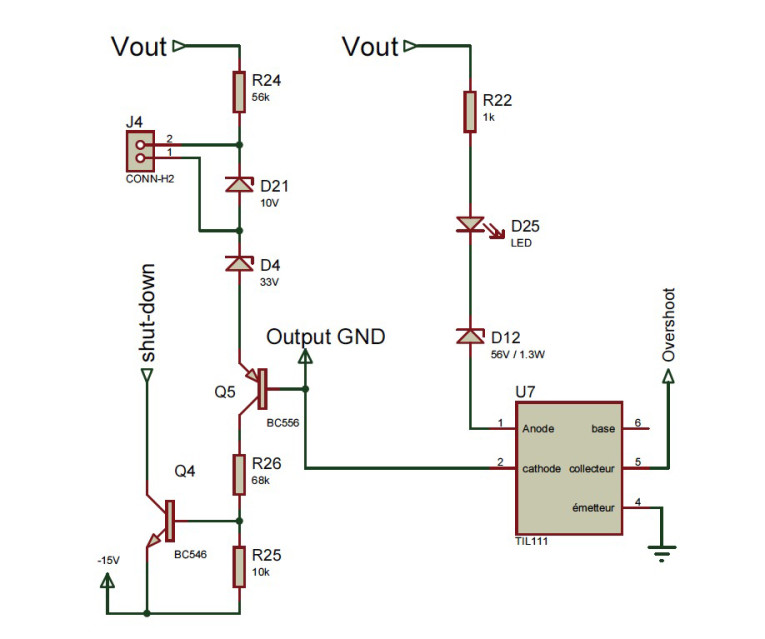
For the nonlinear feedback shown in Figure 6, Ton_max can be lowered by this circuit via shut-down when the output limit is exceeded. The safety circuit is an additional safety measure in case of output overshoot. The LED will illuminate if this occurs.
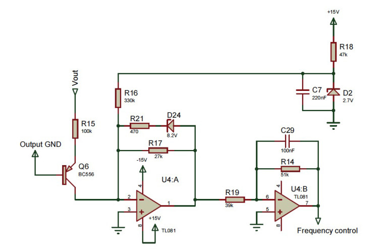
Figure 7 shows the linear feedback, which enables the switching frequency to be proportional to the output voltage, so that the switching structure always works in complete demagnetization mode. This is useful to create a short-time mean output current limitation, while the smoothing capacitors allow output current pulses much higher than this limitation.
Figure 8 shows the power MOSFET driver. The first input is the node of the output regulation. Then you have a first-order low-pass (it has to be slower than half the mains period), a comparator, and a pulse width limiter on which the current limit depends (it is a little wider than Ton_max). The switching MOSFET is driven by 11 parallel gates. Though this is neither scientific nor uses a dedicated specialized driver, it is inexpensive, efficient, simple, and the parts are easily sourced.
DIY Possibilities
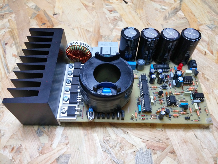
I made an effort to limit the circuit board’s size so I used is a standard 160 × 100 mm circuit board that you can buy. The switching semiconductors are mounted on a power heatsink (3°/W maximum) via a right angle bracket. This right angle bracket must be a minimum 2-mm thick. Note that the efficiency of the power supply gets better when these components get hot.
Warning! This circuit has several limiting and protective features. Nevertheless, you should not reproduce it without basic electronics’ knowledge and experience. Extra care needs to be taken with the components’ orientation, especially the diodes and the capacitors. A buck-boost supply can be very hazardous if you are not careful.
For the First Switch-On
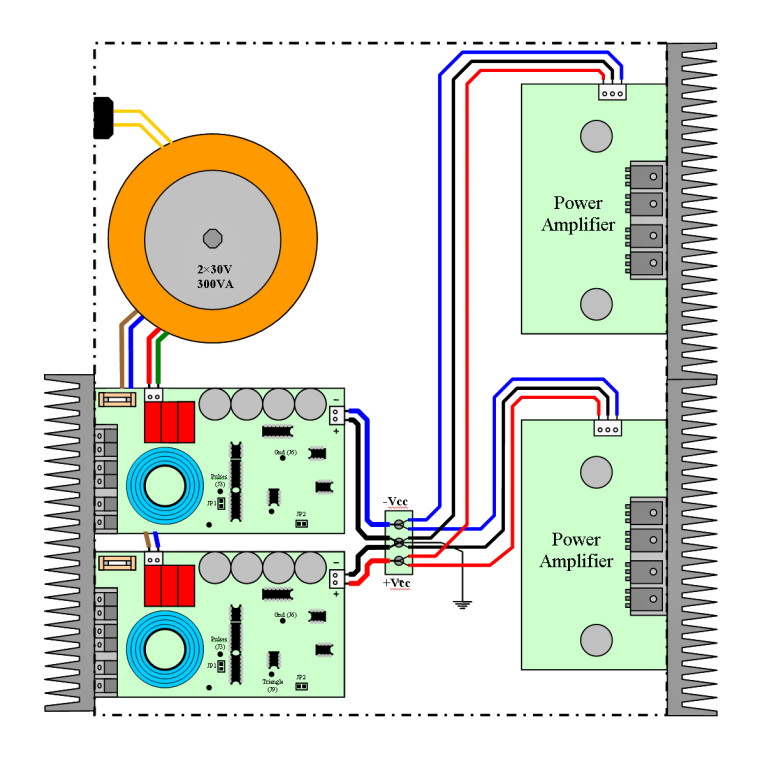
This power supply provides the usual bipolar power supply for your power amplifier. A 2 × 30 V 300 VA transformer is required. There should be no common point between the two secondaries of the transformer. The transformer must have two independent secondaries (see Figure 9). The two power supplies’ outputs are connected in series to get a symmetric bipolar power supply. You may connect or disconnect JP2 to adapt the power supply’s output voltage to the load of the power amplifier—4 Ω or 8 Ω. A 4 Ω load may also require more current. Nevertheless, the power supply has a power limitation so that output voltage and current limitation will adapt themselves to the load when high power is required. Thus, the power amplifier’s heatsinks don’t have to be over-dimensioned as they often are in a classic scheme to take into account a possible 4 Ω load.
Disconnect JP1 at first turn-on and verify the ±15 V outputs. They shouldn’t be lower than ±12 V. Then, verify that you get a triangle wave at the J9 test-point. This triangle wave should swing between 0 V and 5 V. Its frequency can be as low as 1 kHz, but will increase up to 33 kHz once you connect JP1.
Before you connect JP1, verify that you have 15 V pulses at the J3 test-point. These pulses can be as wide as 15 μs. This is because JP1 is still not connected and the regulation allows pulses to be wide for the output voltage to increase.
If everything is okay, shut down, connect JP1, and then power the circuit on again. You will hear a burst-whistling sound. This is the sound of the coil. The lower the output voltage, the lower the switching frequency. As the coil makes more sound through lower frequencies, you will be able to hear it and shows that the output voltage is increasing.
The LED connected to the safety circuit shouldn’t illuminate. But if it does, verify that a small output load current (less than 100 mA) extinguishes it again. If it does not, verify once again that the triangle wave at J9 is correct. If all is fine, your power supply is ready for use.
Comparative Measurements
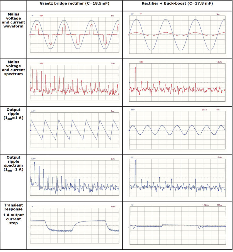
I have taken some measurements to help DIYers test their own power supplies and better understand how it works. They show all the key waveforms of the circuits described in Table 1. Table 3 shows these measurements with the same transformer used in each case, the same smoothing capacitors (4 × 4700 μF), and the output voltage is almost the same (about 42 V). These measurements clearly reveal how much lower the RMS mains current and harmonics are in this new power supply. They also show how much lower the power supply output ripple and harmonic content is with the new power supply.
There will be less impact on your hearing, less irritating 100/120 Hz hum, and less mains harmonic pollution. This power supply requires a lower investment than huge over-dimensioning and expensive shielded mains cables. Low DC impedance will also help get the best out of your power amplifier, whatever it is.
The Results
The measurements attest to the audio benefits of this power supply compared to the classical solution. Its reliability has been tested using four different pieces of equipment — three DIY power amps and a DIY laboratory power supply integrating linear post-regulation. Though I don’t pretend to design better sine wave absorption equipment than the manufacturers, I believe this kind of power supply is real progress when applied to power amplifiers. I hope readers will enjoy building and using this project.
The Gerber files for the PCB and bill of materials for this project are available on the Supplementary Material section of the audioXpress website.
Resource
Linear Audio, linearaudio.net/downloads
About the Author
Vincent Thiernesse was born in France in 1973. He is a teacher in applied physics. He has been an electronics hobbyist since the age of 13. Vincent has written seven articles for the French magazine Electronique Pratique about measuring, audio filtering, and audio amplification. Vincent has a website www.muselec.fr, where you can find some of his audio creations and music compositions.
This project was originally published in audioXpress, June 2016.