A high-quality low-noise preamplifier requires a high-quality power supply, so I used Walter Jung’s regulated power supply as described in his article “Improved Positive/Negative Regulators” (Audio Electronics, 2000). I wanted all the components of the preamplifier and its power supply (except the transformer) to be placed on a single PCB for easiness of the construction. The preamplifier would include an adjustable gain to compensate for the differences a cartridge has between the two channels and optionally a volume control so it could be used to directly drive a power amplifier.
Preamplifier Design
The most important decision for the preamplifier’s design was my op-amp selection. After some investigation, I selected Analog Device’s AD797, which is an expensive single op-amp with bipolar input transistors biased at high collector currents. Considering its ultra low voltage noise (0.9 nV/Hz) and low total harmonic distortion (–120 dB) in audio bandwidth, the AD797 is an excellent choice for a moving coil preamplifier. This preamplifier is especially useful for DIY projects in which quality is the first priority and cost is secondary. Due to its high quality, I decided to use this op-amp in all stages of the preamplifier.
The Preamplifier Circuit
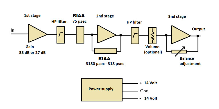
The preamplifier’s simplified block diagram includes the preamplifier circuit and the power supply circuit, which is based on the Jung regulator (see Figure 1).
The preamplifier circuit consists of three stages. The first stage buffers the cartridge and provides two different gains depending on the cartridge’s nominal output voltage. The first high-pass filter comes next and the RIAA equalization time constant at 75 μs follows. These are buffered by the second stage, which also provides the 318-μs and 3,180-μs time constants of the RIAA de-emphasis curve. The third stage buffers the second high-pass filer and the optional volume control, which provides an additional gain between 5 and 7 dB. This can be adjusted with a trimmer to compensate for any possible balance errors between the left and right channels of the moving coil cartridge output. These balance errors are typical for all the cartridges, and in my opinion, should be accurately adjusted.
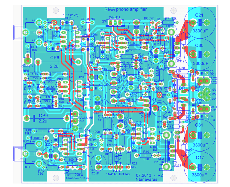
Figure 2 shows the amplifier’s complete electronic schematic. The schematic only shows one channel; however, the other channel is identical. Capacitor CP1 is used to bypass the input ground to chassis. This is needed to suppress any radio frequency (RF) from entering the preamplifier through the input cable’s shielding. Capacitor CP1 should have a good response in the RF spectrum, so I used a 10-nF, 50-V ceramic COG capacitor.
Resistor RP2 and capacitor CP2 adjust the load impedance the preamplifier presents to the moving coil cartridge. They should have the cartridge manufacturer’s recommended values. In the schematic, I used 100 , which is the typical value. The first stage is a non-inverting amplifier based on the AD797. This stage’s gain is defined by the values of the resistors RP3 ad RP4. I tried to keep the resistor RP3’s value as small as possible for minimum noise.
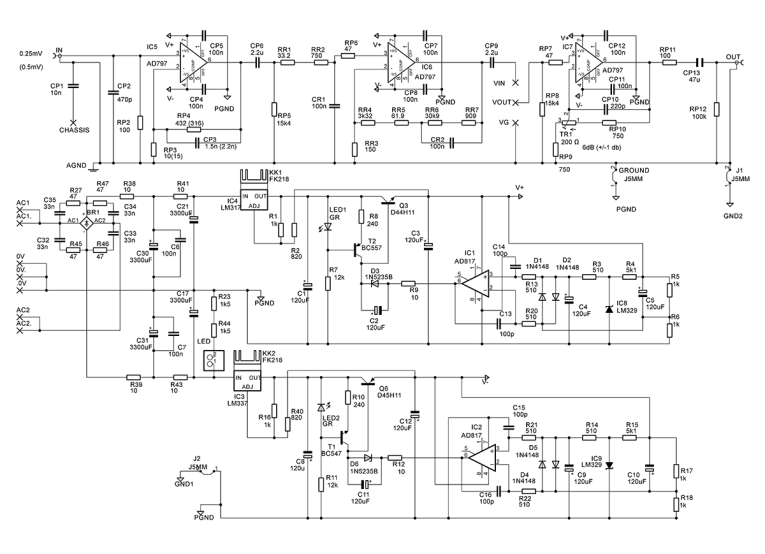
In the schematic, I indicated two possible values for the resistors RP3 and RP4. For a cartridge with a 0.25-mV nominal output, the higher gain should be used with the resistor values RP4 = 432 and RP3 = 10 . These values will give a gain of times 44.2 (32.9 dB). If the cartridge has a 0.5-mV nominal output, then the resistors should be RP4 = 316 and RP3 = 15 . This will provide a lower gain of times 22 (26.9 dB).
Capacitor CP3’s value is also adjusted according to RP4’s value so the high-frequency response’s rolloff will be constant at about 240 kHz for both gain values. CP6 and RP5 form the preamplifier’s first high-pass filter at about 5 Hz. This high-pass filter is required for two reasons. First, you want to prevent any possible offset of the first stage entering to the next stage, which has a very large DC gain.
Second, you need to reject the very low frequencies from the turntable, which may overload the woofer. Resistors RR1 and RR2 and capacitor CR1 form the RIAA equalization first-time constant at 75 μs (2,122 Hz). I used high-accuracy resistors with 0.1% tolerance and a polypropylene capacitor with a 1% tolerance to minimize the circuit’s deviations from the RIAA curve.
The total value of the resistors RR1 and RR2 is somehow larger than the nominal value of 750 because in the PSpice simulations I performed, the high-pass filter of the CP6 and RP5 affects the equalization’s time-constant value and the resistor RR1 has to be added to compensate for this. The next op-amp stage is also based on the AD797 and forms the RIAA equalization’s time constants at 3,180 and 318 μs with the resistors RR3, RR4, RR5, RR6, and RR7 and the capacitor CR2. Here, I also used high-accuracy resistors with 0.1% tolerance and a polypropylene capacitor with a 1% tolerance to minimize the RIAA curve’s deviations as much as possible.
Capacitor CP9 and resistor RP8 form the preamplifier’s second high-pass filter, which is required for the same reasons as the first high-pass filter. Then, I included three pins to connect the optional volume control potentiometer. Any high-quality potentiometer can be used here. However, the total resistor of the potentiometer value in parallel with resistor RP8 should be 15.4-k. If not, the capacitor CP9 should be modified accordingly to keep the low-pass filter around 5 Hz. If volume control is not required, a short circuit between pins VIN and VOUT should be used.
The final stage is again based on the AD797 and provides an additional 6-dB nominal gain, which can be adjusted by ±1 dB with the 200-trimmers. It is absolutely necessary to adjust the gain of each preamplifier’s channel because most of the cartridges I have used do not have the same output signal on both channels. Usually, they differ by as much as 1.5 dB. Use a test record playing the same signal on both channels to adjust each channel’s gain until they have exactly the same output.
Resistor RP11 buffers the amplifier’s output if long cables are connected to the preamplifier. Capacitor CP13 is used to protect the next stage from any possible DC offset that may exist at the preamplifier’s output. This should be a large value capacitor to prevent low frequencies loss so I used a bipolar capacitor.
On my prototype, I used a no-output capacitor since the output offset was less than 1.5 mVDC on the right channel and about 0.2 mVDC on the left channel and the following equipment, that was driven by the preamplifier, was DC protected with an input capacitor. But, be careful! You should use the output capacitor if the line preamplifier or the power amplifier that is going to be driven by this preamplifier is not DC protected with an input capacitor. Otherwise, problems may occur.
The Power Supply
A toroidal power transformer provides the required 2 × 20 VRMS for the preamplifier’s power supply. I used a low-noise 15-VA toroidal transformer with a nominal output voltage of 2 × 18 VRMS with a 230-VRMS input. This transformer actually gave 2 × 20.5 VRMS when it was connected to the preamplifier’s power supply because the required power was much lower.
A 2-A/100-V bridge rectifies the AC voltage to DC voltage and charges the two 3,300-F/35-V capacitors. Resistors R45, R46, R47, and R27, in series with capacitors C32, C33, C34, and C35 are in parallel with the rectifier diodes to reduce their noise.
Resistors R38, R39, R41, and R43 with the reservoir capacitors C30, C31, C17, and C21 form low-pass filters to reduce the ripple voltages of the capacitors. The two regulators are identical to the Jung regulators. Refer the Jung’s original article for further details (see Resources).
A DC voltage above ±19 V should be always kept at the input of the LM317 and the LM337 regulators. This is very important because if the voltage falls below these levels, the regulators will not properly work or they may not work at all.
The transformer I used measured a ±24.2-V voltage at the input of the regulators when the input voltage was at the 230-VRMS nominal value. Keeping in mind the tolerance of the 230-VRMS mains voltage is ±10%, the mains voltage may change from 207 to 253 VRMS. With the mains voltage at 200 VRMS, I measured ±20.6 VDC at the input of the regulators. When the mains voltage went up to 250 VRMS, I measured ±27 VDC.
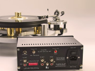
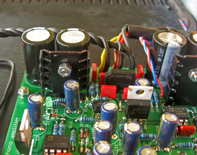
The input voltage at the regulators IC3 and IC4 inputs will vary from ± 20.6 to ±27 VDC, which means they will need some heatsinking to avoid high temperatures on their cases. I used two Fischer Elektronick FK218SA-32 heatsinks, which have a 21°C/W thermal resistance on each regulator (see Photo 2). This was enough to keep them cool even when the line voltage was set continuously to 250 VRMS. I set the nominal output voltages to ±14 V and measured 14.19 and –14.18 V on my prototype.
Amplifier Construction
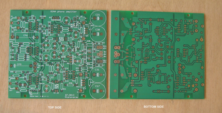
One of the main objectives of this amplifier’s design was to include all its components on a single PCB so the construction would be easy. I used CadSoft’s EAGLE software to design the PCB (see Resources). The one drawback is the demonstration program limits the PCB’s maximum dimensions. The outcome was a 90 mm × 115 mm double-sided PCB with ground planes on the top and bottom layers. I used a separate ground plane for the power supply area.
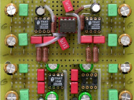
Due to the limited dimensions, each PCB has components for only one channel. Two of these PCBs are needed for the construction of a stereo preamplifier. Photo 3 shows the PCBs, consist of 1.6-mm thickness FR4 board with 35-m copper. Also they have plated through holes, solder resistant on both sides of the board, and silkscreen on the top side.
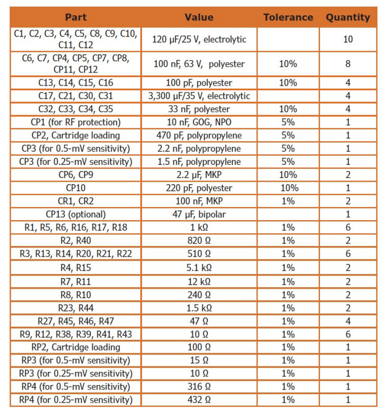
Figure 3 shows the PCB’s complete guide assembly. Table 1 shows the parts list for one channel. I used high-quality parts for the preamplifier’s construction. I separated the signal ground and the power supply ground plane to minimize the noise. They are connected to a single point.
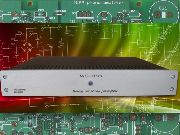
I housed the preamplifier’s components in a metal enclosure with a 10-mm aluminum front panel. The enclosure’s external dimensions measured 330 mm wide × 280 mm deep × 50 mm high. Photo 1 shows the amplifier’s front panel. A single blue LED in the center of the panel indicates the preamplifier’s operation. I used Front Panel Express’s Front Panel Designer program to create the front plate text. Then, I used my inkjet printer to transfer the file to a transparent self-adhesive sheet.
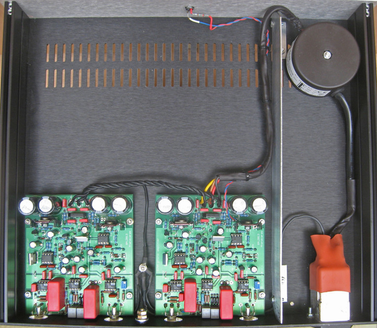
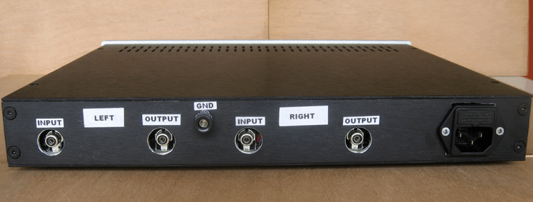
Photo 4 shows an internal view of the preamplifier. Although my first thought was to use a separate enclosure for the transformer, I decided to mount the power transformer on the same box as the gain circuits. I used a quality toroidal power transformer, which, according to the manufacturer, has an extremely low radiated magnetic field and is suitable for sensitive electronics. I mounted it as far as possible from the amplifier’s electronics parts to avoid any possible interference due to the high voltage gains of the preamplifier circuits, especially at the low frequencies. Additionally, I used a metal sheet for shielding between the power transformer and the PCBs to eliminate any possible interference.
The two PCBs were mounted to the back of the enclosure because of the on-board RCA input and output connectors. This means cabling is not required for the preamplifier’s input and output connections. The star point ground is placed between the amplifier’s two PCBs. Here, all the grounds are connected together to the chassis.
Photo 5 shows the amplifier’s back panel. The IEC socket for the 230-V mains is on the right side with an integrated EMI filter. The fuse holder is next to it. On the left side are four large holes for the RCA input and output sockets, which are mounted directly on the PCB. For all the amplifier’s op-amps, I used high-quality IC sockets with gold-plated pins. This facilitates amplifier testing and any repairs that may be necessary. Before inserting any of the expensive AD797 op-amps, check the power supply voltages on pins 4 and 7. They should be ±14 V.
Preamplifier Measurements
After preamplifier construction, I performed the usual measurements to check its performance. First, I measured the preamplifier’s gain at 1 kHz. This was 65 dB with the trimmer 200 turned fully left and 67 dB with the trimmer 200 fully right. The 2-dB margin is more than enough to adjust any balance errors on the output of every moving coil cartridge.
Next, I measured the accuracy of the preamplifier’s RIAA curve. I have an accurate inverse RIAA network, which was constructed with high-accuracy components (0.1% resistors and 1% capacitors), using the ideal values of the schematic diagram (see Resources). Photo 6 shows the network’s enclosure.
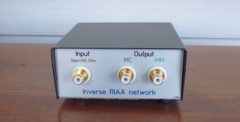
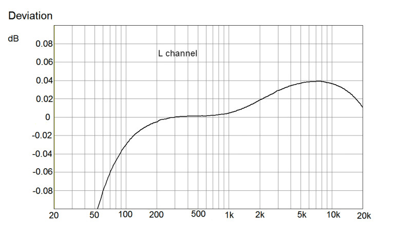
Figure 4 shows the preamplifier’s accuracy with this inverse RIAA network connected at its input. The deviation from the ideal RIAA curve is less than ±0.04 dB from 80 Hz to 20 kHz. Of course, this includes the error of the inverse RIAA network and the MC100 preamplifier.
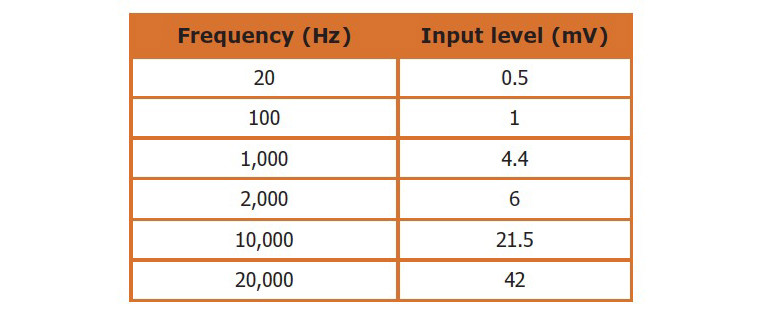
The increased deviation below 80 Hz is intentional and is due to the two high-pass filters used in the circuit to reduce the infrasonic frequencies. The attenuation is –0.5 dB at 20 Hz and –1.8 dB at 10 Hz. The –3 dB point is at 7.8 Hz. Then, I measured the maximum output voltage before clipping at the preamplifier’s output. This was 9 VRMS (12.7 V peak) as expected from an op-amp with a ±14-V voltage supply. Table 2 shows the corresponding maximum permitted voltages in several different frequencies at the preamplifier’s input, which I measured for confirmation.
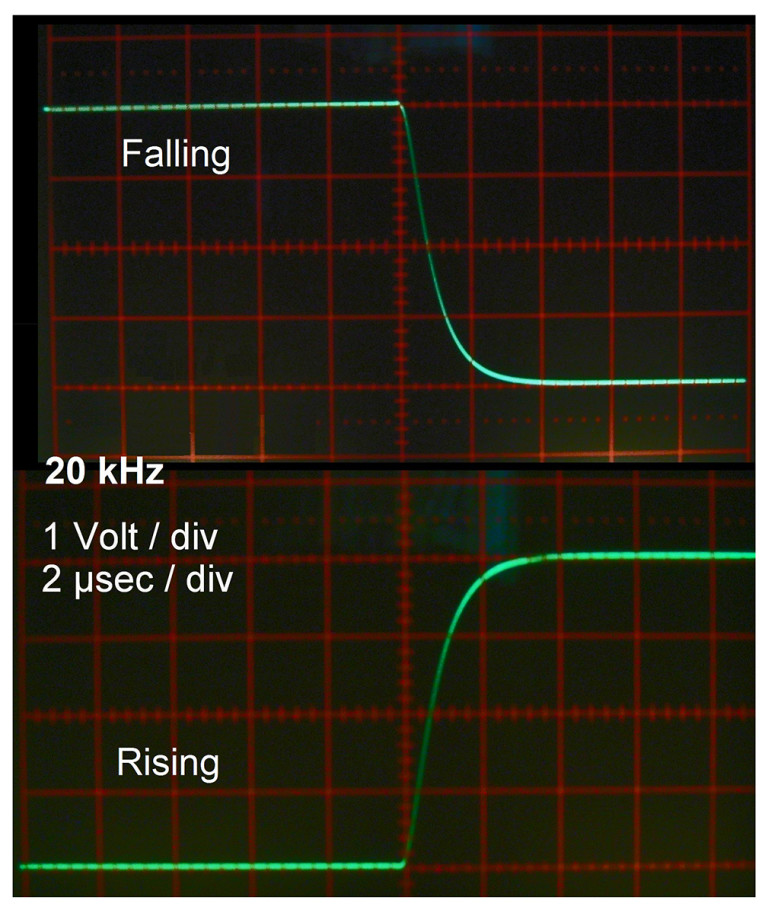
Finally I measured the inverse RIAA network’s response and the preamplifier to a 20-kHz square wave. I connected the generator to the input of the inverse RIAA network and the output of the inverse RIAA network to the input of the preamplifier. Photo 7 shows the excellent response of the preamplifier for the rising and the falling part of the 20 kHz square wave.
Overall Impression
This is an easy to construct high-quality RIAA moving coil preamplifier. It offers an excellent transparency and has a very low noise that is almost undetectable even when my system is set to its maximum volume. If you need such a preamplifier, I think you will enjoy this one. I rediscovered several of my old LPs, and I really appreciate my system’s sound on the quality recordings. aX
This article was originally published in audioxpress, March 2014.
Resources
W. Jung, “Improved Positive/Negative Regulators,” Audio Electronics, Issue 4, 2000.
W. Jung and S. Lipshitz, “A High-Accuracy Inverse RIAA Network,” The Audio Amateur, January 1980.
Sources
AD797 Op-amp
Analog Devices, Inc. | www.analog.com
EAGLE PCB software
CadSoft | www.cadsoftusa.com
FK218SA-32 Heatsinks
Fischer Elektronick GmbH | www.fischerelektronic.de
Front Panel Designs
Front Panel Express, LLC | www.frontpanelexpress.com
About the Author
George Ntanavaras graduated in 1986 from the National Technical University, Athens, Greece, with a degree in Electronic Engineering. He currently works in the Development Department for a Greek electronics company. He is interested in the design of preamplifiers, active crossovers, power amplifiers, and most loudspeakers. He also enjoys listening to classical music.
The author has available a small quantity of PCBs to build the preamplifier.
If you are interested, send him an email by clicking here.