A Quickie Tutorial On FET Amplifiers
One of the aims of these articles is to encourage people to build amplifiers, so here is some tutorial material to get beginners going. I have written up some of this material before (“The A75,” Audio Amateur 4/92), but that was 15 years ago, and maybe it will be helpful to repeat bits of it. All 31 years’ worth can be found at www.passdiy.com and related links.
I’m assuming that you understand the concepts of voltage, current, and resistance. If you already know how a FET works, you can skip ahead. Figure 1 shows an N channel FET, a quantum mechanical black box with three connections. This device is meant to function as a valve, a little bit like a water faucet. In this illustration, the drain (D) of the FET is attached to an electrical power supply, analogous to the pressurized water supply on the other side of the faucet. You can imagine the pipe as wire, and the tank of water as a battery or even a charged-up capacitor.
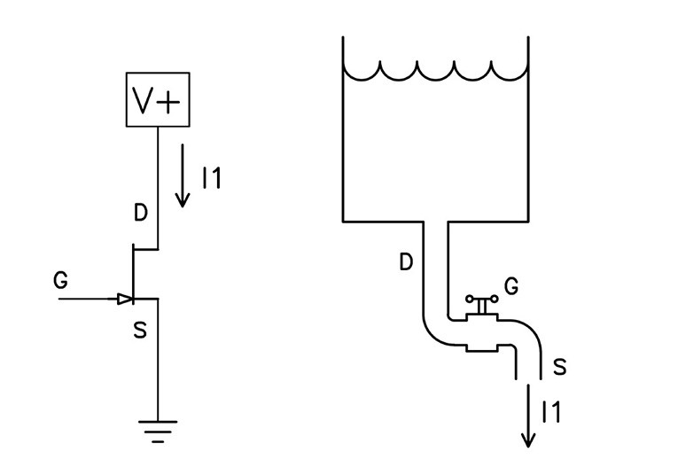
To continue the metaphor, the voltage of the supply is the water pressure, and the water flowing from the supply is the electrical current. The source (S) connection of the FET is the output of the faucet. The gate (G) of the FET is the control pin, and like the handle on the faucet, it controls the amount of electrical current through the FET from the drain to the source. For the FET, this control is a function of the relative voltage between the gate and source pins. For an N channel FET, raising the gate positively with respect to source increases the current flow.
Yes, I know some of you are thinking that maybe the source should be on top and the drain on the bottom, but they’re not. You might not want to call a quantum mechanic if your plumbing stops up. The idea that the current going through the FET transistor is controlled by the voltage between the gate and the source pins remains the key idea, and if you have that firmly fixed, you can leave the waterworks metaphor behind.
FETs come in different types. There are two polarities, N channel and P channel. There are different voltage, current, and power ratings, and different semiconductor processes resulting in JFETs and MOSFETs. In all of them, the current from the drain to the source is controlled by the voltage between the gate and the source. A FET is a three pin device, and there are three ways to amplify with them. Figure 2 illustrates these with an N channel FET:
• Common-Source (CS) is the connection that can give both voltage and current gain in a circuit. The input voltage (shown as a little graphical sine wave) goes to the gate, and the output is taken from the drain and appears across a resistor between the drain and the supply voltage. The source is grounded, and doesn’t show a signal voltage, and that’s why it’s called common-source. Note that the output voltage is inverted
in phase from the input voltage.
• Common-Drain (CD) gives current gain only, and is also known as source follower, because the output voltage across the source resistor is nearly identical to the input voltage at the gate. While the drain is usually attached to a DC voltage value, the AC voltage is ideally zero, and so it is called common-drain.
• Common-Gate gives non-inverted voltage gain only, with the input signal going into the source and coming out the drain. The gate is grounded.
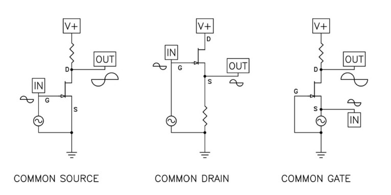
Figure 2 shows what happens only to AC signals, but it doesn’t illustrate the DC voltage and current values that the FETs need in order to operate. These DC values are often referred to as the bias of the device, and you will hear this term a lot with respect to amplifiers. The optimum bias values vary by the device and the needs of the circuit. In general, to function as an amplifier, the FET needs to have at least a few volts between the drain and the source. If the FET is an N channel type, the drain must be at least a few volts positive with respect to the source. If it’s a P channel type, the drain must be negative with respect to the source.
In addition, the gate of the FET must be placed at a DC value relative to the source so that the current and voltage of the FET is positioned in the linear region between the extremes of voltage and current—somewhere between all the way on and all the way off. It is in the middle ground where the distortion is low. Generally for N channel JFETs, it is with the gate voltage at 0 or slightly negative with respect to the source, and for N channel MOSFETs the gate voltage is a couple volts positive. One of the important functions of a circuit is to set up the DC conditions of gain stages so that the devices have stable operation in this region. For every amplifying circuit, there will be a “sweet spot” of voltage and current which will give the best overall performance.
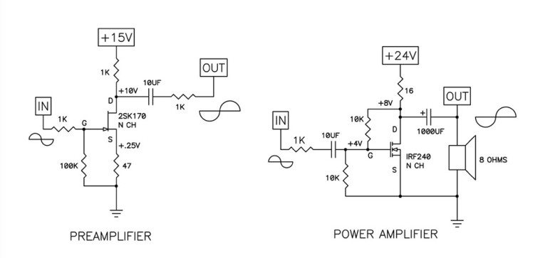
Figure 3 shows some examples of real circuits that illustrate simple common source amplifiers and the bias voltages and currents that would be typical for them. You can build both of these circuits, which will work as shown.
On the left you see an example of a simple preamplifier stage with a gain of roughly 10 times (20dB). The JFET is self-biased in this circuit: With 5mA going through the JFET, the gate needs to be at about -0.25V with respect to the source. Notice 47Ω in series with the source, raising its voltage to +0.25V, which conveniently allows you to bias the gate at 0V DC, or ground.
On the right is a power MOSFET set up as a simple power amplifier, intended to deliver about 1W into an 8Ω loudspeaker. The 16Ω power resistor performs as a current source to the circuit, and the two 10kΩ resistors on the input set the DC value for the gate to about 4V to get it to conduct a 1A bias current. For a more powerful version of this, see Zen Variations #1 (audioXpress, March 2002).
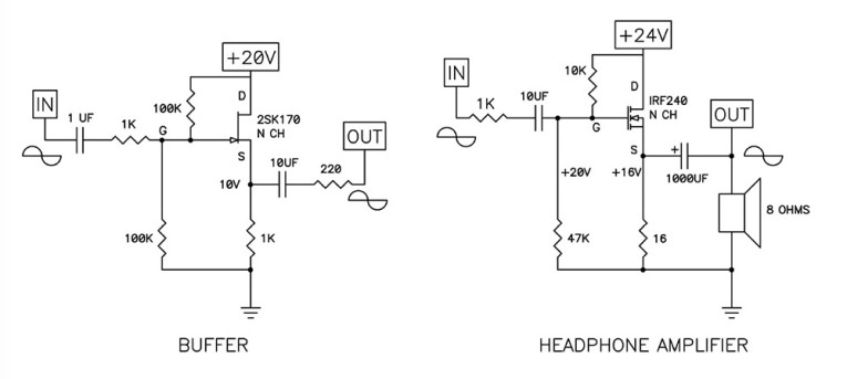
Figure 4 shows some real common drain amplifiers, a line-level buffer that you can use in active filters, and a headphone amplifier. In both cases there is no voltage gain in the amplifier, but there is current gain. They both have high input impedance and low output impedance.
Common-gate operation is encountered less often, usually found in a “cascode” connection with another device. Discussions of cascoding with good examples are found in Zen Variations 8 and 9 (audioXpress, January 2006, May 2006) and also the article “Cascode Amplifiers” originally published in Audio Magazine, March 1978.
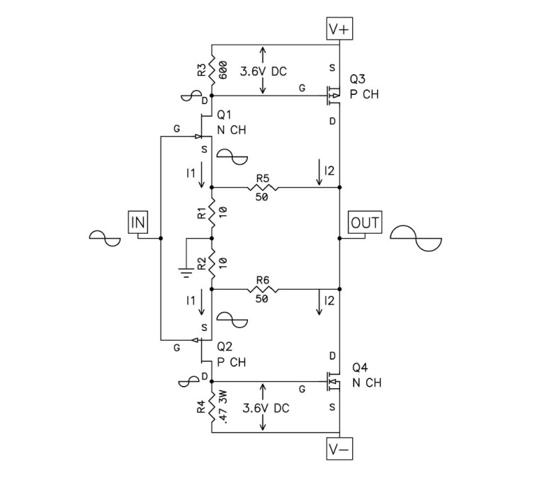
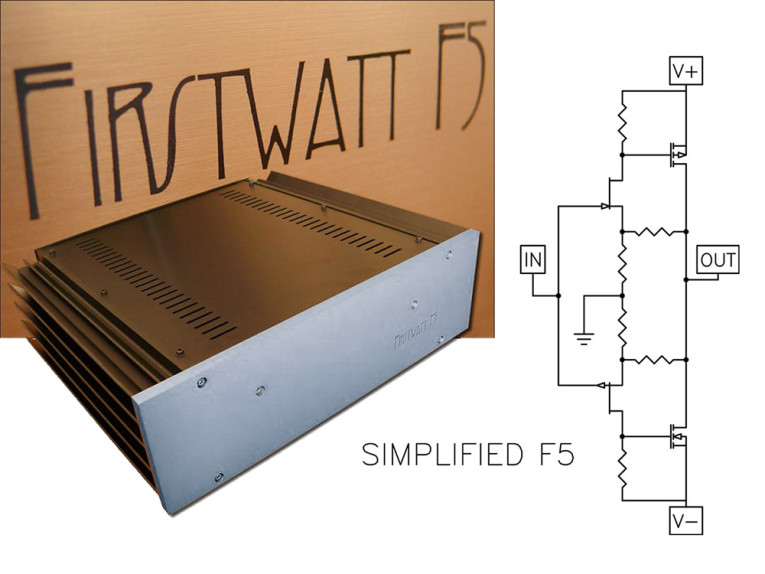
Simplified F5 Circuit
Figure 5 shows the simplest imaginable version possible of the F5. The topology is familiar: a two-stage conjugate complementary circuit using two JFET transistors for the input amplification and two power MOSFET devices for the output. JFETs Q1 and Q2 form a complementary common-source stage, with the input appearing at their gates and output at their drains. The JFETs are class A self-biased at about 6mA, and so a current I1 comes out of their drain connections and produces a voltage of about 3.6V across R3 and R4, whose values are about 600Ω. This 3.6V DC value is necessary to bias the power MOSFETs Q3 and Q4 into conduction.
The voltage gain of Q1 and Q2 appears across each of these resistors for a gain of about 10 each. The gain of 10 for the input stage comes from the ratio of the 600Ω divided by the apparent resistance from the source to ground, which is roughly 60Ω. This 60Ω number comes from the inverse of the JFET’s transconductance plus the 10Ω actual resistor.
The transconductance for a JFET is the ratio of current change against input voltage change. The gain of this part is typically 0.02 siemens, or 0.02A per control volt, and if you invert that you get 50Ω (R = V/I). So it looks as though there is 50Ω inside the part (although there isn’t), and to that you add the 10Ω of the real resistor to get 60Ω.
Q3 and Q4 do the heavy lifting in this circuit, providing the large output current needed to drive the loudspeaker. The DC voltage appearing from the gate to the source of these devices is about 3.6V, and this biases the MOSFETs to about 1.3A. For this sort of circuit, a 1.3A bias means that the amplifier will operate class A to 2.6A of output current. To understand this, imagine a condition in which Q3 and Q4 are idling at 1.3A, so that all the current is going from the V+ voltage rail to the V- voltage rail, and none is going through the loudspeaker.
When a positive voltage appears at the gates of Q1 and Q2, it makes the current through Q1 increase and the current through Q2 decrease. The resulting voltages across R3 and R4 make the current through Q3 increase and the current through Q4 decrease. This makes the output voltage go positive. As the positive input voltage increases, you approach the point at which Q3 is conducting 2.6A and Q4 is conducting 0 amps—and all of the 2.6A goes through the loudspeaker.
The power of 2.6A into 8Ω is I2 * R, or 2.6 * 2.6 * 8 = 54W. This is the peak value, and the nature of an undistorted sine wave is that the peak wattage is twice the average, so this circuit would operate 27W average class A into 8Ω. At currents above 2.6A one of the transistors will shut off, leaving the other to continue to increase beyond the 2.6A in what is known as class AB.
This circuit employs feedback to improve the performance in a number of ways. Feedback sets the gain, lowers the distortion, improves the bandwidth, and produces the output impedance (damping factor) of the amplifier. The feedback mechanism for this amplifier is R3 through R6, a dual pair of low impedance voltage dividers which feed the output to the source
pins of Q1 and Q2. Low impedance feedback has been (incorrectly) referred to as “current feedback,” and it is popular in simple high-speed linear circuits. One of the charms of this arrangement is that unlike the classic two transistor differential pair, the drive current available exceeds the bias of the input stage.
Something different about this example is that each JFET has its own feedback — there are two separate feedback loops to this amplifier, so that the loop of Q1/Q3 is independent of the loop for Q2/Q4. The circuit of Fig. 5 illustrates the basics and does in fact work, but has a tendency toward instability. Local parasitic oscillation is often seen, and the bias drifts with temperature, requiring a lengthy adjustment period. This simplified circuit also has no provision for adjusting against the variations to be seen between real FETs that you will encounter.
Actual Working Circuit
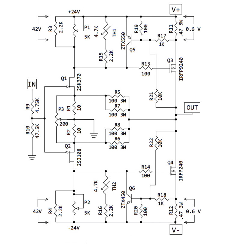
Figure 6 shows a completely functional version of the circuit, with useful enhancements: the addition of R7 and R8 in parallel with R5 and R6 to share the dissipation, allowing inexpensive 3W resistors to do the job. You never know what the amplifier will be attached to, so the input of the amplifier now sports R9 to avoid parasitic oscillation of the input JFETs, and R10 to ensure that the input has a default reference to ground when there is nothing connected.
R11 and R12 are 3W power resistors added to the source pins of the MOSFETs to increase thermal stability and serve as convenient current-sensing elements. R13 and R14 are placed in series with the gates of the MOSFETs to prevent parasitic oscillations, just as you did with R9 on the input stage. R2 and R4 have had their values increased and then placed in parallel with 5kΩ trim potentiometers P1 and P2. This allows adjustment of the output stage bias current and also the output DC offset.
You can stop here, and the amplifier will be fully functional. The remaining additions will enhance temperature tracking and provide for output current limiting. Th1 and Th2 are small 4.7kΩ thermistors placed in series with R15 and R16, respectively. The resistance of the thermistor declines with temperature, and if placed close to the output transistors will help compensate for thermal drift. You can build the amplifier without them, but will have a longer warm-up time and you will spend more time adjusting the bias.
On the positive half of the output stage, Q5, R17, R19, and R21 will arbitrarily limit the output of the amplifier in the event that you accidentally set the bias too high or short the amplifier’s output. Q6, R18, R20, and R22 do the same for the negative half of the amplifier. The output MOSFETs are easily capable of passing very high currents at the request of Q1 and Q2, and it is wise to set a limit in case of accident.
Understanding the limiting circuit is easy. Q5 and Q6 look at the voltages across R11 and R12, and will start to conduct when their base to emitter voltage exceeds 0.4V or so. At 0.4V Q5 and Q6 draw off enough drive current from Q1 and Q2 to start producing measured distortion, and hard limiting occurs when the voltage driving Q5 or Q6 is increased to 0.6V.
Because the 1.3A bias through the 0.47Ω source resistors provides 0.6V already, you must divide that voltage down so that limiting occurs at a higher current. You do this for Q5 with divider resistors R17 and R19, and for Q6 with R18 and R20. R21 and R22 allow you to also adjust the limit point based on some information from the output voltage.
Where do you want to limit? The amplifier with 24 supply rails should be good for a 50W peak into 8Ω, or about 2.5A. For a 4Ω load you would want 5A, and for a 2Ω load, you want 10A. Because you only have two output devices, you probably are best off stopping there.
Calculate the values as follows, starting with arbitrary values of 1kΩ for R17 and R19. At 10A peak, the voltage across R11 or R12 will be about 4.7V. Choose R19 and R21 to divide that down to 0.6V, and solve the formula:
0.6V/4.7V = R19/(R17 + R19)
Because R17 is already 1kΩ, you simplify to 0.127 = R19/(1000 + R19)
And you get R19 = 150Ω
10A into a dead short is about 200W dissipation on an output transistor, which will probably exceed its rating. R21 adds a “foldback” characteristic to this so that the current value will be lower into a shorted output. To ensure against damage into dead shorts, you want to limit the zero crossing current to about 5A, keeping the dissipation just this side of destruction.
Current limiting gets a bad rap in general, but I think it’s a matter of where and how the limits are set. If you build this amplifier, you are, of course, welcome to delete this portion of the circuit, and, of course, you will not complain if a shorted output lets the smoke out of your amplifier. As it is, you will still be taking some chances with a shorted output.
Parts Selection
The input JFETs used are 2SK170 or 2SK370 for the N channel parts (Q1), and 2SJ74 or 2SJ108 for the P channel parts (Q2). In these cases the Idss selection code is BL, although V and GR types can be made to work with adjustments to their drain resistances. The primary thing about these particular parts is the transconductance figure of 20ms—many of the potential substitutes are much lower at 4 to 10ms.
The output MOSFETs are the IRF240 N channel type (Q3) and the IRD9240 P channel type (Q4). They will need a voltage rating in excess of 50V, a current rating of about 15 to 20A, and a dissipation of about 150W. Comparable parts are widely available, and here I used Fairchild FQA19N20C and FQA12P20.
The remaining parts can be generic or special as you see fit. I used Dale RN55D type ¼W resistors and the 3W Panasonic power resistors from Digi-Key, where you can also get the 4.7kΩ thermistors and trimpots. Audiophiles are often concerned about the effects of capacitors in audio circuits, but a quick examination of the schematic will put your concerns to rest.
Power Supply
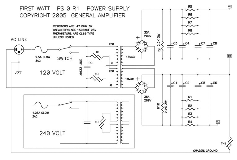
The power supply of the tested amplifier is ±24V and should be rated at 6A continuous duty, and more than 10A peak per channel. Ordinary unregulated supplies will work fine, and if you need suggestions the Zen Variations #5 (audioXpress, October 2003) and Zen Variations #3 (audioXpress, August 2002) both have good examples of regulators and the raw supplies that feed them. I recommend rail voltages from 23 to 25V. (see Figure 15 at the end of the article)
Heatsinking
At 1.3A per channel, you will see idle heat dissipation of 62W. To keep the temperature rise of the heatsink to 20° C above the ambient temperature, you will need a heatsink rated at about 0.6° C/watt for each transistor. An example of this would be a chunk of finned aluminum, with a series of 2″ fins attached to an 8″ × 6″ base. You will need two per channel.
The output devices need to be intimately attached to the heatsink. The mounting surface on the heatsink should be at least ¼″ thick and smooth and shiny. You can use silicone pads for insulation, but Mica and silicone grease are the best.
Initial Adjustment
Before applying power to the amplifier, you must set the values of P1 and P2 to their minimum. Verify this with an ohmmeter. When it comes time to “fire” up the amp for the first time, if you have a Variac, use it, fusing the AC line to the amplifier with a 1A fast blow fuse. Turn the Variac up slowly, and if you haven’t popped the fuse, then go ahead and confirm the rail voltages to the channels.
Each channel does not need to be attached to a load in order to adjust it. If the only load you have is the loudspeaker, I advise against using it during adjustment. For each channel you will be adjusting P1 and P2 alternately in order to achieve 0 volts DC at the output and 0.59V across R11 and R12.
Each time you adjust P1 you will probably need to go back and adjust P2 again, so I recommend adjusting the pots in half-measures, alternately setting the pots half-way to their voltage goals and measuring the DC values. Unless there is something very wrong, when the output is at 0V DC, the values across R11 and R12 will be equal.
In spite of the thermal compensation in the circuit, you should assume that there will be drift as the heatsink temperature rises, and you will need to readjust the values over the course of an hour or two. Usually it is best to start out bias adjustment low, at maybe 0.40V across R11 and R12 until the amp is warmed up a bit.
You should be able to get the output DC offset down to 10mV or so, and I consider 50mV the highest acceptable figure for this amplifier when warmed up. After you have operated the amplifier for a few weeks, it is a good idea to check and adjust the offset again after the parts have been burned in.
Measured Performance
The gain of the circuit is 15dB. The input impedance is 101kΩ, and the output impedance is 0.1Ω, for a damping factor of 80. The noise of a properly laid out circuit is about 30μV with a quiet supply, and raw supply with two 29,000μF capacitors and 70mV ripple will give about 100μV noise (measured in the band from 20 to 20,000Hz).
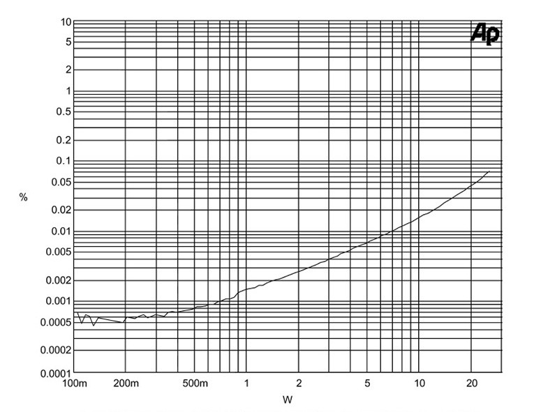
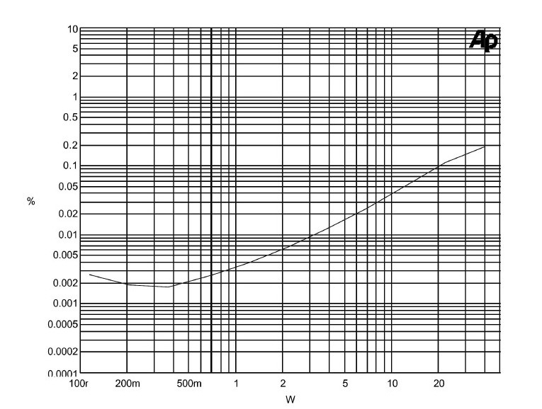
Figure 7 shows the harmonic distortion and noise plotted against output power, taken at 1kHz into 8Ω. This is the lowest distortion yet achieved by either a Zen or First Watt amplifier, descending to .001% below 1W.
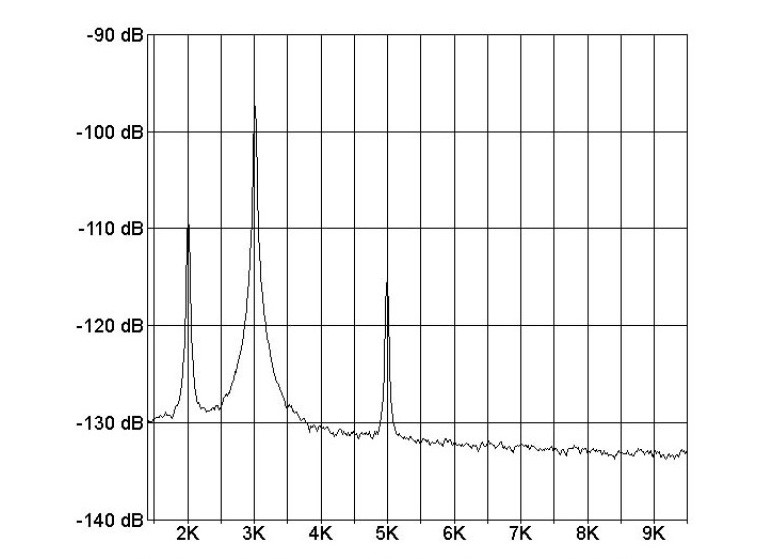
In Fig. 8, spectrum distribution of the distortion at 1W, you can see the dominant 3rd harmonic, as well as 2nd, 4th and 5th. The vertical scale is in decibels relative to 1W. You can also see the noise floor of the system and amplifier at -135dB or so below 1W.
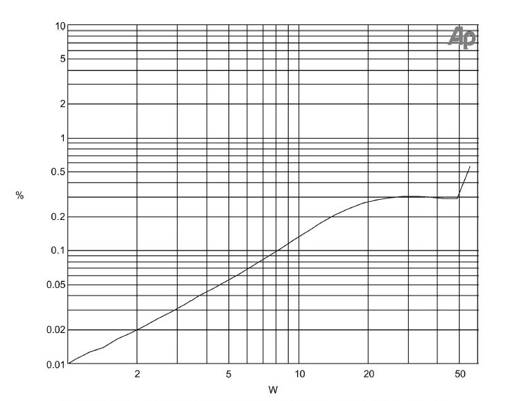
Figure 9 illustrates the harmonic distortion + noise plotted against output power 4Ω load, reaching 0.2% at 40W. Figure 10 shows the harmonic distortion and noise plotted against output power into 2Ω, where the amplifier begins to clip at 0.3% at 50W.
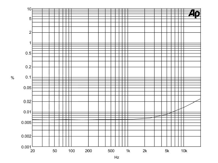
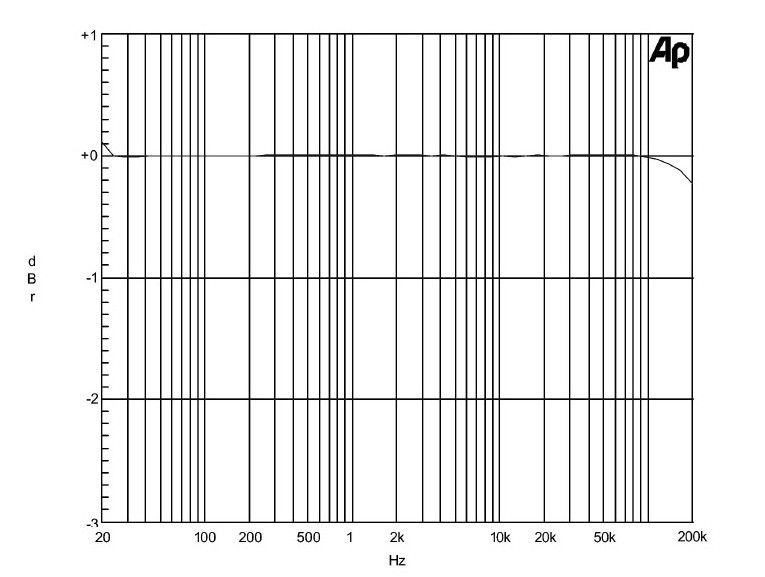
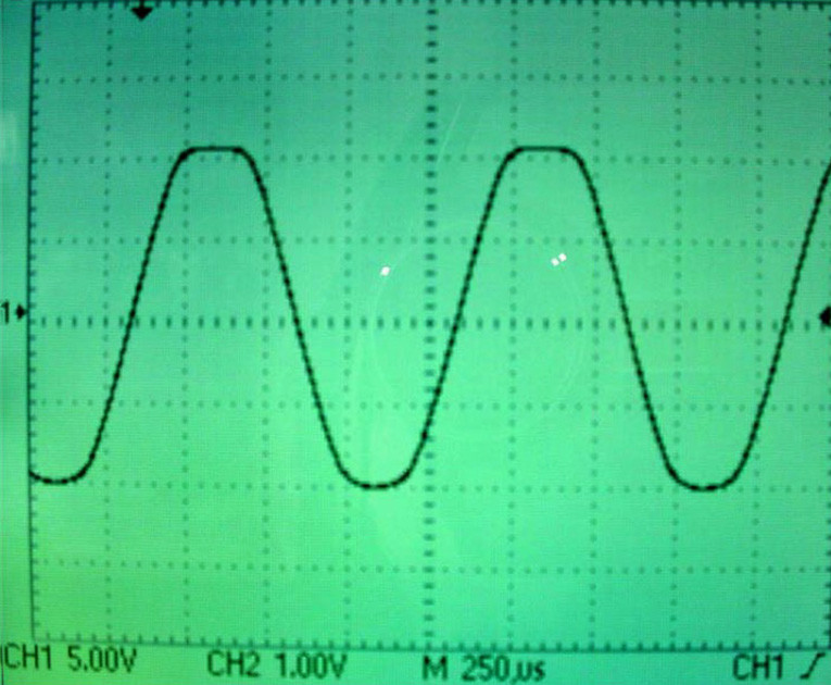
Figure 11 depicts the distortion and noise versus frequency at 2W into 8Ω. Figure 12 displays the frequency response, flat to DC and down -0.25dB at 200kHz. Figure 13 is the square wave response at 200kHz at 1W. The amplifier is flat to DC, and -0.25dB at 200kHz. If you have the equipment to see it, you may find that different gain devices will give you a small peak somewhere just below 1MHz. I have found that you can trim this by playing with the values of R13 and R14, but as both values approach 0 ohms, you are likely to see parasitic oscillations.
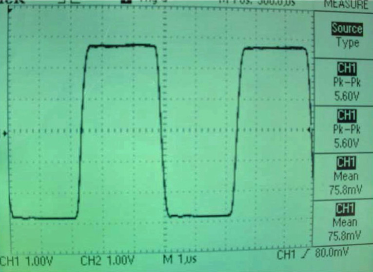
You can additionally limit frequency response with an input capacitor across R10, and also in the feedback loop with capacitance across R5 and/or R8. As you can see, I have chosen not to. Figure 14 shows the behavior of the amplifier clipping into 1Ω at ±10A.
Conclusion
So there you have it, a nice little amplifier without too many parts that sounds great.
Copyright 2008 Nelson Pass - www.firstwatt.com
This article was originally published in audioXpress, May 2008