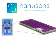
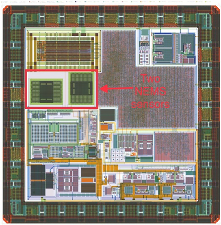
A MEMS (Micro Electro Mechanical Systems) sensor package contains a chip with the MEMS sensor, which is made on the microscopic scale, and a chip with the control electronics resulting in a volume of four cubic millimeters. Nanusens creates its sensors on the nanoscale within the layers of its CMOS chip that also has the control electronics. As a result, the NEMS (Nano Electro Mechanical Systems) chip is only one cubic millimeter allowing to create a saving of three cubic millimeters for every MEMS package that it replaces.
According to the company, headquartered in London, with R&D centers in Barcelona, Spain and Shenzen, China, the more MEMS packages are replaced with a multi-sensor Nanusens chip, the greater the space savings. Plus, the Nanusens chip only increases slightly with every additional sensor function to accommodate additional control electronics. In addition, far less PCB estate is needed for the tiny, single chip solution compared to the PCB estate required for several MEMS packages. All this freed-up space can be used to increase the size of the battery or add a supercapacitor to extend the battery life, one of the key goals among true wireless earbud manufacturers.

As Dr Josep Montanyà, Nanusens CEO and founder, explains, “We are in a unique position of being able to provide more space inside earbuds for designers to use as they wish with our nano-sensors. While some manufacturers want more battery life by using a larger battery or a supercapacitor, others want to use some of this freed-up space for features such as memory so that songs can be stored locally on the earbud. This is another way to extend the battery life as songs would not need to streamed over Bluetooth, again giving longer audio on the go.”
With the current wireless earbud market forecast to grow extremely fast, driven by smartphone manufacturers removing headphone sockets from their designs, the company believes this should provide an important strategic opportunity for Nanusens technology. "New smartphone sales are forecast to be 1.5 billion units a year. As more and more start to ship with a pair of earbuds, our total available market is phenomenal, which is why this is our first target market,” said Dr Montanyà.
“We have started discussions with the leading players in the value chain to make them aware of our innovative technology so that they can start the design-in process,” he adds. “Awareness of a means to significantly increase the battery life of earbuds by the phone and earbud manufacturers will create the pull through the value chain to the Bluetooth chips manufacturers. The latter provide example designs for earbuds that are often used throughout the industry so we are targeting to be in these designs.”
The first product from Nanusens will be a 2D motion detector for earbuds in Q4 2019, which can be used to implement tap and double tap for control, wake-on-movement and sleep-on-rest functions, and, soon after, a 3D accelerometer. A bone conduction sensor for noise cancellation is next to be integrated into the single chip solution. Chips will be available in a small package such as WLCSP or as bare die that can be attached directly to the PCB.
“Our nano-sensor technology is very adaptable so we will be using it to create a range of other sensors,” Dr Montanyà concluded. “These can be created at the same time in the same chip so many different types of sensors can be built into a tiny multi-sensor solution without taking up more space. This provides companies with a roadmap of exciting additional features to enhance the user experience such as controlling the earbuds with head gesture recognition. Our nano-sensors offer a unique combination of significantly smaller solutions, lower power needs, ruggedness, and multi-functionality in a single integrated chip so, after earbuds, we will be bringing our multi-sensor nano-solutions to the wearables and IoT markets.”
Nanusens Nano-sensor Technology
MEMS sensors are created using expensive proprietary processes. Nanusens’ multi-patent pending technology enables it to create nano-sensors inside the CMOS layers using standard CMOS processes within the same production flow as the rest of the chip production. This innovative approach reduces the size and cost of the sensors. Nanusens believes that its disruptive technology will revolutionize the sensor market and meet the ever-increasing demand for lower cost sensors in smartphones, wearable technology and IoT devices that has already made sensors a multi-billion-dollar industry as they provide the vital interface between the real world and the electronics.
The nanoscale of this technology means that it has ultra-low power consumption. Importantly for a sensor in a device that is likely to be dropped, the NEMS design is more robust and reliable than MEMS designs.
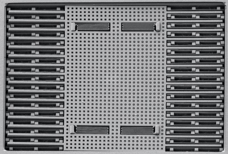
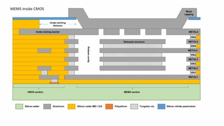
The Inter Metal Dielectric (IMD) is etched away through the pad openings in the passivation layer using vapour HF (vHF) to create the nano-sensor structures. The holes are then sealed and the chip packaged as necessary. As only standard CMOS processes with minimal post-processing are used and the sensors can be directly integrated with active circuitry as required, the sensors can potentially have high yields similar to CMOS devices. This also means that the production is fab-independent.
Founded in 2014 by Dr. Josep Montanyà, Dr. Marc Llamas, and Dr Daniel Fernandez, Nanusens leverages the research and expertise developed by the founders’ previous company, Baolab Microsystems. Nanusens will be showing this technology solution at MWC 2019 on booth 6M14 in Hall 6.
www.nanusens.com